-
Updated 2023-07-12: Hello, Guest! Welcome back, and be sure to check out this follow-up post about our outage a week or so ago.
You are using an out of date browser. It may not display this or other websites correctly.
You should upgrade or use an alternative browser.
You should upgrade or use an alternative browser.
Serious proposal: accelerator and peripheral expansion system
- Thread starter ZaneKaminski
- Start date
ZaneKaminski
Well-known member
Like a splitter that makes two PDS slots from one? If the ethernet card uses DMA (I think many of the SE/30 ones do), I think there would need to be a bit of logic on the board to arbitrate between the two cards for memory accesses. If both cards assert /BR (bus request) at the same time, some logic on the PDS splitter must then ask the 68030 on the SE/30 to use the bus, and then grant the bus request to only one of the cards. A round-robin or more complex priority scheme can ensure that both cards have the opportunity to access main memory. Heh, a splitter could have some SRAM cache memory on it, too, so it would act like a cache card.A cheap SE/30 adapter for a Daystar card + connector for Ethernet would make my day.
Okay, I'm just dreaming about the cache stuff, but I think other than that, the adapter can be, electrically, straightforward. Mechanically it might be difficult to ensure fitment, but the shape and size can just be copied from another card with the same function. (PDS splitters for SE/30 exist, right?)
What machine do you have? And what peripherals are you using?I need my NuBUS slots. I'm already short 1 slot.My vote is for PDS.
Trash80toHP_Mini
NIGHT STALKER
If you have the proposed IIci version of this accelerator, you'll not necessarily require the Rocket. If the proposed IIci accelerator can be accessed under RocketShare, that would be a different kettle of fish and very cool indeed!
What you're thinking of would likely be the PDS splitters for the Macintosh IIsi.
Dual functions in a single NuBus slot (Video and NIC) are present on some Futura Video cards.
edit: dunno if it might be helpful, but you can see traces on the Radius 16 Accelerator for the SE in the HiRes pics posted in applefritter's NuBus Mafia gallery. Info on slot decoding/interfacing for your card might be apparent.
Not that I know of offhand, SE/30 cards have passthru connectors and stack vertically for the most part. PowerCache adapters for the SE/30 appear to me to place the accelerator in a horizontal position with the PDS passthru set up for vertical stacking as normal. The ARTMIX adapter places the accelerator connector vertically and has horizontal mounting provision for a PDS card as far as I can tell from pics online.(PDS splitters for SE/30 exist, right?)
What you're thinking of would likely be the PDS splitters for the Macintosh IIsi.
Dual functions in a single NuBus slot (Video and NIC) are present on some Futura Video cards.
edit: dunno if it might be helpful, but you can see traces on the Radius 16 Accelerator for the SE in the HiRes pics posted in applefritter's NuBus Mafia gallery. Info on slot decoding/interfacing for your card might be apparent.
Last edited by a moderator:
olePigeon
Well-known member
The Rocket accelerates my video card. Also, it's just damn cool. Mine has 128MBs of RAM and I do launch RocketShare on occasion for giggles.If you have the proposed IIci version of this accelerator, you'll not necessarily require the Rocket. If the proposed IIci accelerator can be accessed under RocketShare, that would be a different kettle of fish and very cool indeed!
ZaneKaminski
Well-known member
I've just redone the clock system, and fixed a problem with some of the level shifters. The way I was doing the /BG and /BGACK signals would have been way too slow for operation at 8 MHz. Maybe 2 or 5 MHz max. So I fixed it. While doing that, I managed to add the ability for the card to function as either a PDS master (accelerator) or slave (expansion card). And better, it can do both at once, in the sense that it can run the emulated 68000 while also letting the main Macintosh run too, making it similar to the Rocket in the sense that you can have a slow Mac and a really fast Mac going at once. Again, not something I want to implement myself, but a cool area to be developed in the future.If you have the proposed IIci version of this accelerator, you'll not necessarily require the Rocket. If the proposed IIci accelerator can be accessed under RocketShare, that would be a different kettle of fish and very cool indeed!
Ah, yes. Hmm. I'd like to add a passthrough connector for my eventual SE/30 card, but it may make the unit too costly. Paralleling the PDS slots is really frustrating. And anyway, I'd wanna add another set of 3 $2.50 FPGAs on the other side to talk to the card you attach. That would help with throughput. Adds a ton to the cost though. Just fantasies at this point. Let me focus on SE and Plus. I know exactly how I'm gonna do the 68000 emulation. 68030 is not as clear, and, especially when MMU emulation is enabled, will be slower than 68000 emulation.Not that I know of offhand, SE/30 cards have passthru connectors and stack vertically for the most part. PowerCache adapters for the SE/30 appear to me to place the accelerator in a horizontal position with the PDS passthru set up for vertical stacking as normal. The ARTMIX adapter places the accelerator connector vertically and has horizontal mounting provision for a PDS card as far as I can tell from pics online.
What you're thinking of would likely be the PDS splitters for the Macintosh IIsi.
I love the early Radius stuff. One question, though. What is the separate ROM board for?edit: dunno if it might be helpful, but you can see traces on the Radius 16 Accelerator for the SE in the HiRes pics posted in applefritter's NuBus Mafia gallery. Info on slot decoding/interfacing for your card might be apparent.
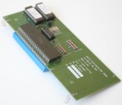
It's got its own 68000 (10 MHz grade), and then the 68020 board goes on top:
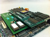
So there are two 68000s in this system and one 68020? Trash, do you know anything about this?
Edit: that's different from the board you linked though. That one seems to be installed in a Plus.
Amazing. I have been wanting one since I was 12 hahah. Do you have any technical description of the Rocket? I would be dying to read it and make sure Rocket acceleration is possible to implement with my design.The Rocket accelerates my video card. Also, it's just damn cool. Mine has 128MBs of RAM and I do launch RocketShare on occasion for giggles.
Last edited by a moderator:
Trash80toHP_Mini
NIGHT STALKER
That the pic was of the original Mac Plus version of the card was my first guess. Mine was the Radius 16 for the SE as in the NuBus Mafia's HiRes pics, no additional ROM necessary. WAG would be that the ROM board bypasses (disables with an INIT?) the 68000 on the Mobo, its 68000 booting from the expanded (?) ROM on board and then the Accelerator's 68020 bypasses that.So there are two 68000s in this system and one 68020? Trash, do you know anything about this?
Edit: that's different from the board you linked though. That one seems to be installed in a Plus.
I wonder if it's like a double Rocket WHOOSH taking place without the attendant sound effects?
This is the card that turned me into a Radius collector, the Macs are almost incidental, LOL!
Solder Side of Radius 16
Component Side of Radius 16
credit: applefritter/NuBus Mafia
I'd like to get a look at the mounting hardware Radius used before the advent of the Killy Klip?
ZaneKaminski
Well-known member
Yeah, Radius's socket thing that sits on the 68000 looks really promising.
I wonder why they had to have a second 68000 though. I guess this accelerator must predate some software present in the rom to hand off control to an accelerator. I will have to investigate this further.
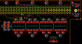
Here's some more progress on the SE board:
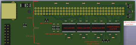
Here's how it looks in KiCAD (this shot taken a little earlier):
I wonder why they had to have a second 68000 though. I guess this accelerator must predate some software present in the rom to hand off control to an accelerator. I will have to investigate this further.
Here's some more progress on the SE board:

Here's how it looks in KiCAD (this shot taken a little earlier):

Last edited by a moderator:
Trash80toHP_Mini
NIGHT STALKER
Nice! I do my board layout in rev 9 of Adobe Illustrator on G4s under OS9, LOL! I've etched my own boards since Illustrator 88 was the bees knees so that's really no biggie. SMT might wind up a bit tricky at some point with my old masking methodology, but so far I don't think so.
I'm curious about the (assumed) need for meandering traces on paleolithic hardware. At what clock rate would a trace length differential of about a meter actually become problematic? Interpolating from that value for different system bus speeds would be interesting.
< wonders if he should mention the trusty Wire Wrap tool in the workbench carousel? : >
>
I'm curious about the (assumed) need for meandering traces on paleolithic hardware. At what clock rate would a trace length differential of about a meter actually become problematic? Interpolating from that value for different system bus speeds would be interesting.
< wonders if he should mention the trusty Wire Wrap tool in the workbench carousel? :
ZaneKaminski
Well-known member
That's crazy! I've never heard of doing them in Illustrator. Most of the boards I work on have 50+ components. I think this board will have around 120 :\. So the EDA program is important. KiCAD is actually a pretty crappy program, but it's the best free EDA/CAD program so I've gotta use it for the Maccelerator. Have you ever seen KiCAD in use on a classic Macintosh? Apparently it's been around since 1992, originally for Macintosh only.
I've also never personally etched a board. Wire-wrap stuff, I used to, but not since I became good enough at bringing up a microcontroller in a design. Now I can just trust myself to do the board right the first time. They're dirt cheap nowadays anyway. Almost all of mine are 4 layers too, Maccelerator-SE included. Nothing beats a solid reference plane for routing ease and signal integrity. I've tried ground grid schemes, but they all require you to do the thing where you route the traces on top in one direction, and the other direction on the bottom. Guess I'm too young for that type of routing hahahah.
In terms of timing skew, at 8 MHz, I would say a meter of lengthwise skew is fine, but not great. Rule of thumb is that signals propagate at half the speed of light on FR-4. So that's around 6.6 nanoseconds, out of 125 for the whole cycle at 8 MHz, or about 19 degrees out of 360. Not great but not terrible. Obviously it depends on the timing specs of the chip, but 19 degrees isn't that much for SDR. Most of the 68000's timings at 8 MHz are specified in tens of nanoseconds, so it's not that bad. The level shifters I'm using impose a similar delay, but of course that's evenly across all of the signals so I wouldn't call it skew as much as just propagation delay.
I'd say that a bigger problem with such a long trace is that it might radiate a lot of emissions unless you keep it close to ground or whatever the return path is.
Edit: Naturally, these few nanoseconds are a bigger deal for a 68030 accelerator. For 68030 Macs, the maximum bus speed is 25 MHz, right? (On IIci, as I understand IIfx has a 20 MHz bus.) At 25 MHz, the timing budget of a design similar to the current one becomes more strained. 6 ns or so for input to come in from the level shifters, some time for the FPGA to do its stuff, maybe as much as 10 ns, another 6 ns to get the output through the level shifters. So that's 22 ns latency, more than half of a clock cycle. So maybe the current design will have to be tweaked somehow. There are some ways of improving the latency, so I don't think it will be a problem, but may be a source of greater cost.
Last edited by a moderator:
Trash80toHP_Mini
NIGHT STALKER
LOL! Crazy I am, but PCB layout started out as and remains art to me so I've used what I've had. The first one I did with a sign making package in '89 so I could cut silk screen stencils for enamel ink resist for a few protocards at a time or to cut and use the vinyl lettering stock itself as resist for a quickie!. No Gerber files (the vinyl cutter was a Gerber machine though : ) involved back then. I cut rubyliths at 400% for reduction on the board house's copy camera for the production run! Olde schoole!
Using illustrator has been a breeze in comparison to that start. I recently got some Laser Print resist sheets on eBay and I can't wait to give that a try. My board layout/prototyping is hobby/hacker level at this point. All I want to do is mess around with PDS and memory bus cards just for shiggles and gits. Illustrator is fine for things as simple as that and the artwork is prettier too! [ ] ]'>
] ]'>
IIfx system bus and CPU are both 40MHz! On just a 20MHz PDS Card or memory bus I figure an inch, or maybe even two inches difference between the longest and shortest traces won't matter over lengths under 10 or 12 inches.
I snagged a boxed copy of PowerPCB from one of the comrades here to give that a try sometime. That'll run under Win98 along with the yet to be used ROM burner I still need to figure out. Heh!
Using illustrator has been a breeze in comparison to that start. I recently got some Laser Print resist sheets on eBay and I can't wait to give that a try. My board layout/prototyping is hobby/hacker level at this point. All I want to do is mess around with PDS and memory bus cards just for shiggles and gits. Illustrator is fine for things as simple as that and the artwork is prettier too! [
IIfx system bus and CPU are both 40MHz! On just a 20MHz PDS Card or memory bus I figure an inch, or maybe even two inches difference between the longest and shortest traces won't matter over lengths under 10 or 12 inches.
I snagged a boxed copy of PowerPCB from one of the comrades here to give that a try sometime. That'll run under Win98 along with the yet to be used ROM burner I still need to figure out. Heh!
Trash80toHP_Mini
NIGHT STALKER
Dunno if this may be of any use: last sentence in this post . . .
. . . or maybe this: another of techknight's musings.
Gotta love the ways the guy's wetware works! :approve:
. . . or maybe this: another of techknight's musings.
Gotta love the ways the guy's wetware works! :approve:
Last edited by a moderator:
Trash80toHP_Mini
NIGHT STALKER
Not so much, I'm a visual thinker and the only time I did a layout for over 50 components was the first and they were all DIP CMOS at about the time Don Lancaster wrote that designing a board without a MicroProcessor on board was becoming counterproductive. My brain doesn't do schematics or much electronics for that matter. So board design to me is an exercise in electron plumbing and a visual schematic development process.That's crazy! I've never heard of doing them in Illustrator..
/monthly_05_2014/post-902-0-53226400-1399000094.jpg">View attachment 2884
Here's the most recent example of that schematic development (simple as it is) by visual electron plumbing in a piece of artwork. It's probably gobbledegook to you, but that's the way my head wraps around the schematic development you do so effortlessly.
Hand routing from scratch beats tweaking an autorouted layour or unscrambling a rats nest for something this simple any day of the week. FWIW, my brother (Blade packaging designer ME) has a good friend who does the heavy duty, high speed multi-layer PCB design for a living and for whatever reason, he's in awe of my process for simple, home etched two sided protoboard/schematic development. Not absolutely sure if that reaction's horror, amazement or some combination thereof, but he smiles enthusiastically and it works for me! [
edit for a bit of clarity: top half of PCB on its own converts the banks of what should be 30 pin 16MB SIMMs (dream on!) for my Quadra 950 into a much more economical pair of 32MB 72 pin DIMMs using simple 30 pin SIMM SIP header adapters as the interboard connections. The bottom half of this layout pairs that with another pair to replace the 4MB of soldered ICs hobbling Bank A in my IIsi with a DIP ground interleaved ribbon cable soldered at the business end to various points on the IIsi MoBo. Like I said, it's a hobby!
Last edited by a moderator:
ZaneKaminski
Well-known member
Hm. 40 MHz is pretty fast. I’ll make sure all 68030 cards are good up to 40 MHz bus clock, in case someone tries to apply an adapter to use it in an IIfx. I’ll also only use signals common to all 68030 machines, so any adapter should work. I really wanna do a multifunction NuBus video card instead though, with support for basically any monitor. Shouldn’t be too hard with a programmable PLL to multiply a slow clock to make the pixel clock for any display.
thetechknight was going in a good direction with the FPGA and 68000 soft core. I rejected that approach because none existed supporting '020 instructions. The coprocessor idea he was describing is good but if it's gonna have a fancy ARM system, why not just do it all on there.
And this is key to achieving the 50x speedup over Plus or SE or whatever I claimed I could do. When you run a core in an FPGA, you don't get a fancy cache system with a few Mbytes of L2 and tens of kbytes of L1 cache, which you get in an ARM SoC. The FPGA could probably only accommodate a small L1 cache, and then maybe you could add external L2 SRAM, but... that quickly becomes too complicated, and it doesn't work as well when the L2 cache isn't on-die. The ARM cores are already great at cache management and branch prediction and all that other stuff that a good processor must do. Combined with translating the M68k code into ARMv8-A instruction such that register-register operations don't touch memory of the ARM chip, that makes for a really fast emulation solution. Even if there is double or triple indirection involved in emulating a memory access or jump, the ARM processor is just so fast compared to anything you can make in an FPGA, so it doesn't matter.
The portable accelerator is hard in terms of getting it within the power budget. Maybe an ARM Cortex-M7 running an interpreter, with a bit of SDRAM and an FPGA accessible through the MCU's external bus interface would provide a small boost to a Portable. That would probably still exceed the power budget for the Portable's PDS, but only barely. Even the fastest Cortex-M7 available is only 400 MHz though, and they don't accommodate hundreds of megabytes of SDRAM, so the emulation would probably have to be strictly interpretive emulation, no translation, no fancy peripheral emulation, no USB, etc. But it would be possible, and cheap compared to what I'm doing. Slower though.
I understand what you’re saying about the schematic design. Relatively little time is spent doing schematic capture compared to board design, so as the hardware matures, I always find myself thinking about the circuit more in terms of the board than the schematic.
Your board is cool. I like the idea. But will it work electrically? The skew shouldn’t be that bad, but at 25 MHz and 5 V, I think your board may end up radiating a lot of radio emissions. All of your traces are perpendicular on the top and the bottom, so that’s good (reduces crosstalk), but you should try and consider how the return current flows. You wanna minimize the “loop area” of the entire trace by laying it next to or twisting it with ground. This is why I was saying earlier about having a solid GND plane underneath each trace. It helps a lot as you exceed 15 or 20 MHz. Indeed, it may be useful to you to pair two of the etchable two-layer boards together, with the signal traces on the outside, and a solid GND plane on the inside. You could pair GND and a power plane together too if you put some kind of dielectric in between. The thinner the better, since then you turn the board itself into a capacitor, which is helpful for signal integrity. I’d also stick some capacitors on your board between power and GND.
More progress on SE card:
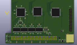

Trash80toHP_Mini
NIGHT STALKER
Thanks, your input is much appreciated, even if the "electrically" part and terms are over my pay grade. I do know enough to dump overall board capacitors and bypass caps for the DIMMS as the design progresses. My first board was a header connected pair of boards about the size of a full length ISA card and then a third adapter board was added the size of a short card. It worked great at what I think was 8MHz. SIMMspenders for the IIsi are 20 MHz stock or 25MHz reclocked to Apple's original design spec, but the Quadra version would have to work at 33MHz.
Your board is coming along nicely, can't wait to see more! Doing a NuBus VidCard sounds like a great time. I'll have to dig up one of my old threads about an amazing SuperMac card from 1989, you'll LOVE it!
Your board is coming along nicely, can't wait to see more! Doing a NuBus VidCard sounds like a great time. I'll have to dig up one of my old threads about an amazing SuperMac card from 1989, you'll LOVE it!
Trash80toHP_Mini
NIGHT STALKER
About the power budget for the Portable's PDS: ISTR reading a spec that an external power source was required. Just checked DCaDftMF2e and there's no mention of it there. Hrmmm? Have you considered decoupling the Power pins and jumpering from 5V on one of the peripheral interconnect cables. A M-F adapter for the cable ought to be easy enough to knock out.The portable accelerator is hard in terms of getting it within the power budget. Maybe an ARM Cortex-M7 running an interpreter, with a bit of SDRAM and an FPGA accessible through the MCU's external bus interface would provide a small boost to a Portable. That would probably still exceed the power budget for the Portable's PDS, but only barely
About NuBus: if you haven't run across mention of it, bbraun has done a bit of work on the NuBUs slot's interface to DECLROM. IIRC, that's about as far as he got with the project so far, he's into so many things. His Mac68k development site id down for maintenance ATM, but it would be worth a look when it's back online.
About NuBus VidCards: take a look at info in the SuperMac Spectrum/24 Project That sucker is likely the most flexible, if not the only RAMDAC level user configurable VidCard made in Mac NuBus. It predates full implementation of Mac specific Video resolutions so it's implementation intentionally provided a fully open playing field. [
techknight
Well-known member
dont worry about the Portable's power issues. I have ways around that.
ZaneKaminski
Well-known member
The bus stuff I have right now is applicable to the Portable, but I've encountered a little problem. I'm not 100% sure that the FPGA implementing the Control Glue has enough capacity.
The Control Glue must not only implement the M68k bus control, but also implement an asynchronous interface to the Snapdragon, which will report certain signals (e.g. /RESET, /IPL[2..0]) and allow for the submission of commands (e.g. "read word with FC=001," "acknowledge interrupt"). It must also report the result (in terms of success, failure) of the most recent M68k bus operation.
The Address Glue and Data Glue FPGAs share the asynchronous bus (to the Snapdragon) with the Control Glue and they must be loaded with the desired address (for all M68k bus operations) and data (for write operations only, for read operations the data is retrieved from the Data Glue before the operation command is given to the Control Glue. The Address Glue and Data Glue may seem to have little more function than a latch, but they are both designed to either output data or latch data incoming from the Mac. This enables the accelerator to function as a memory-mapped peripheral. In addition, the Address Glue can be programmed with some address decoding logic when the accelerator is set up to emulate a memory-mapped peripheral. That allows the Address Glue to tell the Control Glue to assert /DTACK. Also, for 68030, the Data Glue must sort of rearrange the data according to /DSACK[1..0] or SIZ[1..0] in order to accommodate the variably-sized 68020/'030 bus.
So the Address Glue and Data Glue are well-matched to the capabilities of the MachXO256 FPGA I've chosen, I would say, but the Control Glue functionality seems like it may not fit into the MachXO256, which has 100 pins and costs just $2.25. Maybe it needs the more capacious MachXO640, also with 100 pins, but that costs $6.50 or so, raising the total FPGA cost from $7 to $11. At that point, it would be better to use the MachXO1200, with 144 pins, to implement the Control Glue and Address Glue. It costs maybe $7, making the total cost under $10. Combining the Address Glue and Control Glue would yield certain performance benefits as well. Unfortunately, no cheap FPGA has enough pins to combine all three. I was looking at a $12 Cyclone IV with 208 pins, I think, but its total cost to implement would be greater than using these MachXO units.
Last edited by a moderator:
ZaneKaminski
Well-known member
Does the PB100 have a PDS? I can't find the 68000 on its motherboard. Is the 68000 on a card?
Last edited by a moderator:
Similar threads
- Replies
- 0
- Views
- 173
- Replies
- 42
- Views
- 2K
- Replies
- 14
- Views
- 556
- Replies
- 7
- Views
- 653
- Replies
- 49
- Views
- 3K
