• Updated 2023-07-12: Hello, Guest! Welcome back, and be sure to check out this follow-up post about our outage a week or so ago.

Reverse-engineering the Lapis ProColorServer 8 II

Arisotura

Well-known member
I figured I might as well make a thread for this video card, as it piques my curiosity.
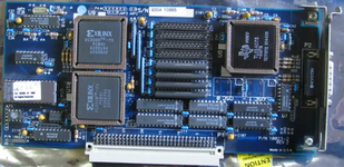
Lapis-ProColorServer-8-II-NuBus-Card-Apple-Macintosh.png

I did get that card a while ago, but didn't do much with it at the time. Reason was that I couldn't really get it to work with much.

I looked into it again lately. It does work with one of my monitors, which happens to support sync-on-green, except most of the time the picture is tinted green, and the monitor may have trouble aligning it properly. It doesn't work at all with my other monitor which doesn't support sync-on-green (and seems pickier about sync signals in general).

This card outputs sync on green, but it also outputs separate H/V sync signals. I found out that if I cut off these separate H/V sync signals, I reliably get a perfect picture on my SoG monitor. So I figured that what's happening is that my monitor is picking up the H/V sync instead of the green sync, but the H/V sync this card produces are weird and causing these issues.

I also have a Macintosh II color video card, and that one does work fine with both monitors (and apparently anything really). It does also output sync on green, but I guess the H/V sync it outputs do closely match the green sync so things work out.

This piques my interest, and I kinda want to see what it would take to make the Lapis card VGA-compatible. Also, the way this card is made in general does make me want to see what's possible.

The main components of the card are:
* Xilinx XC3030 and XC2018 -- FPGA chips
* Texas Instruments TLC34075 -- video interface chip with palette
* VRAM
* NuBus ROM
* support chips (bus transceivers, timing generation, etc)

The Xilinx chips don't hold any configuration data on their own, and have to be configured at startup, which is where things get interesting.

A while ago I dumped the NuBus ROM for this card. The ROM appears to contain 8 possible sets of configuration data for the Xilinx chips. Each set is 0xB00 bytes long, and they start at offset 0. Then at offset 0x6000 we get the DeclROM stuff and the initialization code for the card.

So it appears that this card has different possible modes of operation, which is interesting.

I want to figure out how the various components map to the NuBus interface next. I'll prolly post findings in this thread. If anything, I like figuring out how things work.
 

Arisotura

Well-known member
I found out that the chip at U13 isn't an op-amp or something of that kind, it's a Xilinx XC1736 -- a serial configuration PROM. It holds the configuration for the XC2018.

I whipped up a quick Arduino sketch to dump the contents of that PROM. I attached the dump if that's of interest. I stored MSb first, LSb last, this bit order seems to be backwards compared to what's in the NuBus ROM.

Now it all makes sense. I did some probing and tracing, and found that the NuBus ROM's address lines are connected to the XC2018 (and not directly exposed to the NuBus interface), so clearly the XC2018 has to be configured before the NuBus ROM can be accessed.

I have yet to determine all the functions that the FPGA chips fulfill. The XC3030 is involved in addressing the VRAM, that much I know.
 

Attachments

  • LapisPCS_PROM.bin
    4.4 KB · Views: 2

Bolle

Well-known member
The XC2018 implements the Nubus control logic, the XC3030 is the video controller including line/row counters, DRAM controller for the VRAM and depending on how the TI palette/DAC interfaces to the VRAM it will also act to shift video data to the TI chip.
The different 3030 configurations in the Nubus ROM are for different video modes and they're loaded accordingly either through a specific driver or while primary init runs and determines the state of the sense lines on the video connector to figure out what resolution and sync frequencies it has to use.
One of the two FPGAs will also handle communications with the programmable frequency generator that's on there.
 

Arisotura

Well-known member
Thanks for the info! You seem to have already done some work with this card, that's interesting!

BTW I provide a version of the PROM dump with the same bit order as what's in the NuBus ROM (LSb first, MSb last). I figured it makes more sense this way.
 

Attachments

  • LapisPCS_PROM.bin
    4.4 KB · Views: 3

Arisotura

Well-known member
I worked out most of the connections.

I quickly made a list for the connections to the FPGA chips. There's still a bunch of unknowns there.

I found Ken Shirriff's XC2064 reverse-engineering work, which is going to prove interesting here. The XC2018 is basically a scaled-up version of the XC2064, it contains 10x10 logic blocks instead of 8x8, but other than that, it's the same basic thing.

The XC2018 here handles the address decoding logic. A lot of it seems trivial (the address outputs for the ROM are simply the NuBus address lines inverted), but I still need to work more on it and hopefully figure out how the various components are mapped inside the NuBus address space.

As for the XC3030, I don't know yet how I'll go about it. It's a different family, it has 10x10 logic blocks like the XC2018 but the hardware is different and has more features -- the bitstream for it is longer than the XC2018's.

The XC3030 only seems to control the address lines for the VRAM. The TLC34075's pixel input port directly connects to the VRAM chips' serial output ports: P0-P7 go to bank 0, P8-P15 go to bank 1, and so on (I consider each two chips to be a 'bank'). This suggests that populating the higher VRAM banks might enable true-color mode, according to the way the TLC34075 accesses memory.

Interestingly, while the TLC34075's VSYNCOUT is passed directly to the monitor output, HSYNCOUT is passed through the XC3030.
 

Attachments

  • lapis_connections.txt
    3.3 KB · Views: 5

zigzagjoe

Well-known member
I worked out most of the connections.

I quickly made a list for the connections to the FPGA chips. There's still a bunch of unknowns there.

I found Ken Shirriff's XC2064 reverse-engineering work, which is going to prove interesting here. The XC2018 is basically a scaled-up version of the XC2064, it contains 10x10 logic blocks instead of 8x8, but other than that, it's the same basic thing.

The XC2018 here handles the address decoding logic. A lot of it seems trivial (the address outputs for the ROM are simply the NuBus address lines inverted), but I still need to work more on it and hopefully figure out how the various components are mapped inside the NuBus address space.

As for the XC3030, I don't know yet how I'll go about it. It's a different family, it has 10x10 logic blocks like the XC2018 but the hardware is different and has more features -- the bitstream for it is longer than the XC2018's.

The XC3030 only seems to control the address lines for the VRAM. The TLC34075's pixel input port directly connects to the VRAM chips' serial output ports: P0-P7 go to bank 0, P8-P15 go to bank 1, and so on (I consider each two chips to be a 'bank'). This suggests that populating the higher VRAM banks might enable true-color mode, according to the way the TLC34075 accesses memory.

Interestingly, while the TLC34075's VSYNCOUT is passed directly to the monitor output, HSYNCOUT is passed through the XC3030.
I'll be curious to see if you make any headway on those FPGAs.

I took a look at the XC3000/XC3100 FPGAs used on the Carrera 040 with an eye towards reverse engineering, but the best case scenario I found was if you managed to obtain the original proprietary software you'd merely be able to see the gate level view without any additional info to help understand it.
 

Jockelill

Well-known member
Bolle has rev
I'll be curious to see if you make any headway on those FPGAs.

I took a look at the XC3000/XC3100 FPGAs used on the Carrera 040 with an eye towards reverse engineering, but the best case scenario I found was if you managed to obtain the original proprietary software you'd merely be able to see the gate level view without any additional info to help understand it.
Bolle has reversed the Carrera 040, so definitely doable 😅
 

zigzagjoe

Well-known member
Bolle has rev

Bolle has reversed the Carrera 040, so definitely doable 😅

He's reversed the schematics, GALs, and FPGA bitstream - I used what he posted to make my own Carrera.

However, as far as I'm aware the actual gate level function of those FPGA bitstreams remains a black box (think GAL equations). What I've heard is the only folks that can do that kind of reverse engineering aren't sharing the tools.
 

maceffects

Well-known member
I have the Verilog emulation of a NuBus video card, however, 12v <> 5v and PCB design for it is beyond our skill level.
 

Jockelill

Well-known member
He's reversed the schematics, GALs, and FPGA bitstream - I used what he posted to make my own Carrera.

However, as far as I'm aware the actual gate level function of those FPGA bitstreams remains a black box (think GAL equations). What I've heard is the only folks that can do that kind of reverse engineering aren't sharing the tools.
Ah, gotcha , yeah, that would be truly awesome. Long time ago when I was at the university and had a course in computer science we did play a lot with fpga and also had a simulator for it, but not sure the reserve is easily doable. Basically you would want a true emulator for the FPGA which you could feed with the dumped bitstream. Xlinx most certainly had some kind of tool for it, but probably lost in time…
 

Arisotura

Well-known member
Lil' update on this.

I've been looking at the XC2018 stuff, but I'll need to work on making sense of the more complex logic. I have some bits of it figured out though.

I'm also starting to look into the XC3030. Figured out some bits here and there, still a lot to go. The good thing is that barring the edges, most of the chip follows the same pattern, and I have the basic bitstream layout down, so figuring everything out shouldn't take too long. Will likely depend on how much time and motivation I have.

In the meantime, looking at the init code gives us some theoretical insights on the NuBus address space mapping.

FD6001: TLC34075 registers (one every 4 address bytes)
FD7001: ?
FD7003: ?
FD7800: XC3030 config data input
FE0003: DeclROM (one ROM byte every 4 address bytes)

Each of the XC3030 profiles contains 4 extra bytes which are 34 03 1D 13 (except for one of them, where it is 04 03 1D 13). These are likely init values for the TLC34075 registers. They are written to FD6021 and up, which would be TLC registers 8..11.
 

Arisotura

Well-known member
Fun thing I just noticed. When I created this thread, I pulled a picture of the Lapis PCS from a quick Google search, mostly because I was lazy. I looked back at it yesterday, and it turns out that the card in the picture is mine.

Other than that, I was thinking about all the FPGA stuff.

Basically, what I did for the XC2018 was take Shirriff's code and adapt it to the XC2018, and add route tracing code. The code I added is a bit of a mess, but it does the job -- given any output line (such as the input from a pin, or a CLB's outputs) it is able to figure out which inputs it's connected to, and provide path data that can be visualized, as well as a list of destination points. Basically reconstructing nets from the raw bitstream.

This is workable for the simpler stuff -- a bunch of the incoming NuBus address lines are simply NOT'd and forwarded to ie. the DeclROM, the XC3030, ... But there are also big clumps of logic that handle NuBus transfers and address decoding, and these are harder to work through just by hand.

I just had the idea of turning this visualization tool into an emulator of sorts. I do have experience with emulating more complex systems (my main project is a DS emulator, for example), but I've never done something like this. Basically I'd want to feed it a list of inputs and see what the outputs look like, as well as the internal state during the simulation. I already have code in place to resolve the routing, I would just need to add in stuff like clock lines, and obviously reproducing the CLBs' functions and stuff.

I'm also looking into the XC3030. From what I'm seeing, the routing seems more straightforward, but the CLBs and IOBs have more features. I'm currently working out the switch matrices at the edges.

I will probably put it up on Github or somewhere, this may be interesting for other reverse-engineering projects.
 

Melkhior

Well-known member
This is workable for the simpler stuff -- a bunch of the incoming NuBus address lines are simply NOT'd and forwarded to ie. the DeclROM, the XC3030, ... But there are also big clumps of logic that handle NuBus transfers and address decoding, and these are harder to work through just by hand.
NuBus isn't very complex, except for the multiplexed bus aspect that may requires latching the address. Burst mode is a bit more complex, and so is bus-mastering, but I wouldn't expect.a video card to need either. Burst isn't implemented by the host on Mac II and just as slave for Quadras, so is limited to device-to-device on MacII and also device-to-host on Quadras. Bus-mastering is mostly for data-incoming devices, though in theory could be used for QD acceleration as well (don't know that any cideo card but the 8*24GC ever did anything with any of that).

Card ID decoding seems external to the FPGA form your pin mapping, as it doesn't have access to A24-A31, and the NuBus device must compare A28-A31 to ID0-ID3 to check if it is the target. There should be some device in there doing that and telling the FPGA.

It's also not connected to any of the bus-mastering stuff - I expect the ARB[0..3] signals from NuBus aren't connected to anything?

I had a small TB to test NuBus from vivado when debugging NuBusFPGA, but it"s quite primitive and I'm not a HW guy so not sure if it can help. There's also the XiBus implementation I originally used that could inform your analysis, my branch is here (it's pure verilog whereas my own NuBus FSM is in Migen or LiteX).
 

Arisotura

Well-known member
The card ID is checked by U12 (8-bit comparator), one side of it connects to the address lines and the other to the NuBus ID lines, then the comparator output goes to the XC2018. Also, iirc, the comparator is connected to A24..28, which would mean this card only supports standard slot space.

I haven't found any connects to the ARB0..3 lines, indeed. Makes sense, as far as I can tell the Lapis PCS is a simple framebuffer card and it isn't able to initiate transfers.

Thanks for the info tho. That'll prolly come in handy for the things I have in mind, we'll see.
 

Melkhior

Well-known member
Also, iirc, the comparator is connected to A24..28, which would mean this card only supports standard slot space.
Does it not check A[28..31] at all for slot ($F) vs. super-slot ($9-$E) area? In theory that's needed as otherwise the superslot area of other devices could be accidentally matched... (for instance the NuBusFPGA can map all of the on-board memory in the superslot area for the RAM disk). Not that the superslot area saw much use, but still. A[24..27] are indeed needed then when A[28..31] == $F for the specific slot area... but then maybe they used some other tricks, as saving hardware wherever possible reduced costs.
 

Arisotura

Well-known member
I'd need to look at it again when I'm back home, but I think A28..31 are compared against ground (which would be a $F given the NuBus address lines are inverted).
 

Arisotura

Well-known member
Status update.

I added an emulator of sorts to the XC2018 visualization tool I have, which seems to mostly work. There are probably still details to work out. I'm thinking of putting it up on Github, could be interesting.

I also made progress on the XC3030 front. I figured out all the switch matrix connections, the CLB settings, the connections in the middle region of the chip (where it's essentially the same pattern copypasted a bunch of times). I still have work to do on the edge and corner regions, but I'm going to take a break first.
 

zigzagjoe

Well-known member
Seconding the extreme interest in your FPGA work... If you can crack the XC3030, I imagine the rest of the X30xx/X31xx series would fall in line
 
Top