-
Updated 2023-07-12: Hello, Guest! Welcome back, and be sure to check out this follow-up post about our outage a week or so ago.
You are using an out of date browser. It may not display this or other websites correctly.
You should upgrade or use an alternative browser.
You should upgrade or use an alternative browser.
Reverse-engineering the Lapis ProColorServer 8 II
- Thread starter Arisotura
- Start date
cheesestraws
Well-known member
Anything you do feel able to put on github / out there would, I'm sure, be fascinating. I'd encourage it 
Arisotura
Well-known member
I think I can put up my XC2018 work on Github today, will just need to clean up some tidbits. I could even put up a demo of it on my server. It would include my emulator thing -- the labels and definitions I added to that are for the Lapis PCS, but they can be changed in the code to match whatever you need.
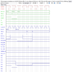
Here's a screenshot of the emulator for example. The way it's set is to run one CLKIN0 cycle with default inputs, then feed the provided inputs for one cycle, then revert to default, basically simulating a NuBus transfer. It shows how the various outputs behave, like here for example we see that feeding an address of $FD6021 activates TLC_RD (pin 46). Note: the address inputs are normally active-low, I made it invert them automatically so they're readable. The address outputs are active-high, but not all bits are output.
As far as the XC3030 is concerned, I was thinking about it, and I want to take a bit of a different approach. Shirriff's XC2064 tool was pretty much tailored to the XC2064. For example, the way it knows what each bit in the bitstream is, is a huge text file defining each single bit. I was able to extrapolate it to the XC2018 but it was quite a bunch of work. I'll want to take a more scalable and less hardcoded approach for the XC3030, so it could be reused for other FPGAs of the XC3xxx family.
Here's a screenshot of the emulator for example. The way it's set is to run one CLKIN0 cycle with default inputs, then feed the provided inputs for one cycle, then revert to default, basically simulating a NuBus transfer. It shows how the various outputs behave, like here for example we see that feeding an address of $FD6021 activates TLC_RD (pin 46). Note: the address inputs are normally active-low, I made it invert them automatically so they're readable. The address outputs are active-high, but not all bits are output.

As far as the XC3030 is concerned, I was thinking about it, and I want to take a bit of a different approach. Shirriff's XC2064 tool was pretty much tailored to the XC2064. For example, the way it knows what each bit in the bitstream is, is a huge text file defining each single bit. I was able to extrapolate it to the XC2018 but it was quite a bunch of work. I'll want to take a more scalable and less hardcoded approach for the XC3030, so it could be reused for other FPGAs of the XC3xxx family.
Arisotura
Well-known member
I put up the XC2018 stuff on Github, over here: https://github.com/Arisotura/xc2018
The demo is available here: https://blargcity.kuribo64.net/xc2018/ (https://blargcity.kuribo64.net/xc2018/emulator.html for the emulator)
I also attached a .rbt of the XC2018 bitstream for anybody interested.
I'll keep you folks updated on the XC3030 front, too. It seems XC3-family FPGAs are relatively common in old Mac hardware, but I dunno about the XC2 family.
Attachments
Arisotura
Well-known member
The .rbt file is a text version of the raw bitstream. You get whatever comment lines at first, then a 40-bit preamble, then the data frames as required for your FPGA, then 4 stop bits. You can open a .rbt file in Notepad and it's lines of 0s and 1s.
If you know the frame length and number of frames for your FPGA (they're in the datasheet) and if you can code, it isn't hard to convert a raw binary dump to .rbt form. Alternately, I could look into supporting raw binary files in the visualizer/emulator.
If you know the frame length and number of frames for your FPGA (they're in the datasheet) and if you can code, it isn't hard to convert a raw binary dump to .rbt form. Alternately, I could look into supporting raw binary files in the visualizer/emulator.
zigzagjoe
Well-known member
Here's a powershell script I wrote to validate the Carrera bitstreams from a binary file and convert into a bitstream file.
Basic algo is for each binary byte, convert to 0/1, and reverse bits in each byte. If there is only one FPGA in the file then I believe this would produce exactly what @Arisotura code is looking for.
Basic algo is for each binary byte, convert to 0/1, and reverse bits in each byte. If there is only one FPGA in the file then I believe this would produce exactly what @Arisotura code is looking for.
Code:
$bytes = [System.IO.File]::ReadAllBytes($inFile)

$bitStream = ($bytes.ForEach({
    $bits = [Convert]::ToString($_,2).PadLeft(8,'0').ToCharArray()
    [array]::Reverse($bits)
    $bits
}) -join "").Trim()
Attachments
Arisotura
Well-known member
I quickly added support for raw binary files. But hey, that would work too. You'd just need to add linebreaks to separate each data frame.
Edit- I quickly looked at the Carrera bitstream you attached. Turns out it contains two bitstreams in one -- one for a XC3020 and one for a XC3042. Interesting. That means they have daisy-chained the two FPGAs there.
I didn't think of that possibility. I'll have to see what I could do, there.
Here's the file with newlines added.
Attachments
Last edited:
zigzagjoe
Well-known member
Yep - two FPGAs, one directly connected to the ROM, the other is daisy chained with the first's DOUT pin. My understanding is the master (3020) accepts the data out of the PROM and once it's fully loaded begins clocking bits out of DOUT which goes to the second's DIN.I quickly added support for raw binary files. But hey, that would work too. You'd just need to add linebreaks to separate each data frame.
Edit- I quickly looked at the Carrera bitstream you attached. Turns out it contains two bitstreams in one -- one for a XC3020 and one for a XC3042. Interesting. That means they have daisy-chained the two FPGAs there.
I didn't think of that possibility. I'll have to see what I could do, there.
Here's the file with newlines added.
The powershell script has the parameters for length and frame size for each as I was validating the format while DIY'ing a programmer.
Bolle
Well-known member
Wow, that was quick indeed. Just right when I figured out how to convert my files. Just dragging them on is much easier thoughI quickly added support for raw binary files.
The layout it produces seems indeed to be pretty accurate. From what I can tell by comparing the schematics for the accelerator I'm working on at the moment with the layout of the inputs and outputs on the XC2018. For example it handles connection of the cards (D*) data bus to the PDS data bus (DB*):
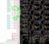
Input from data bit 0 from the PDS ends up on bit 16 of the card and vice versa. The same is true for the rest of the data bus.
The logic does make sense as well as far as I can tell.
The only thing that's a bit awkward is when you want to trace back an input to a CLB. Clicking on it only highlights the outputs.
Arisotura
Well-known member
Oh yeah. The way I originally did the tracing was to start from an output and find all connected inputs. I could look into adding backtracing for inputs. The tricky part is that the tracing data I generate includes all connected inputs, so ideally I'd need to exclude those that aren't relevant.
Also, by the way, you can right-click CLBs to see their logic. It is likely that the bus lines are going to be buffered, that's what happens in the Lapis PCS.
Edit- nevermind I somehow forgot that that line in the screenshot isn't going through any CLB
Also, by the way, you can right-click CLBs to see their logic. It is likely that the bus lines are going to be buffered, that's what happens in the Lapis PCS.
Edit- nevermind I somehow forgot that that line in the screenshot isn't going through any CLB
Last edited:
Bolle
Well-known member
Yeah, already know that you can right click the cells from Kens implementation for the XC2064.Also, by the way, you can right-click CLBs to see their logic. It is likely that the bus lines are going to be buffered, that's what happens in the Lapis PCS.
Edit- nevermind I somehow forgot that that line in the screenshot isn't going through any CLB
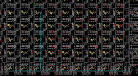
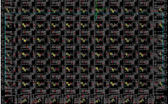
The data bus lines are all just bidirectionally going from one I/O to another with a logic cell controlling the output enable for each direction individually:
Everything that's connected is relevant though, unless I'm misunderstanding.The tricky part is that the tracing data I generate includes all connected inputs, so ideally I'd need to exclude those that aren't relevant.
Arisotura
Well-known member
If you're tracing from an output pin, you'll want to find all the input pins that are connected to it, yeah. But if you're tracing from an input pin, I think you want to know which output pin connects to it, so ideally you'd want just that. Unless I'm mistaken.Everything that's connected is relevant though, unless I'm misunderstanding.
Also, your bitstream makes use of IOB clocks, which is interesting. Mine doesn't use them, so I didn't add support in the emulator -- might change that if need be.
Arisotura
Well-known member
Status update: I finally finished mapping out the XC3030 bitstream. The only thing missing is the misc configuration options like TTL/CMOS, pullup, ...
Now I need to code the visualization tool. I have some ideas to make it adaptable to the entire XC3 family. I might backport it to the XC2018 tool to make it also support the XC2064 (and make the code easier to deal with -- the route tracing code is a mess atm).
I'm also thinking about how I could take this further. Maybe make the emulator more configurable, maybe output netlists in some useful format.
Arisotura
Well-known member
Lil' status update.
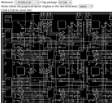
I mostly finished making this view. It's largely algorithmic so it adapts to all the XC3000 family layouts. Only things is that the XC3020 has some subtle differences and I'll need to make sure these are supported correctly, and XC31xx family chips have a few extra interconnects that I haven't added yet.
The chip package option changes the labels on the I/O pads. Smaller packages may have unconnected pins, like the U77 above. The IOB circuitry still exists and is functional (and might be used for nifty tricks), it's just not connected to any physical pin.
What is showing so far is just the background layer -- there's another superimposed canvas layer that will serve to render actual info like paths, config, ... I intend to add options to the view so all the background mess could be hidden away, but right now it's serving to ensure I laid out all the paths correctly. The path system I added will also let me do tracing in a more efficient way -- the code I had added for that in the XC2018 viewer was a big mess.
Now I 'just' have to parse the bitstream and render it in a sensible way.
Arisotura
Well-known member
Bit of a status update. Maybe at some point I should make a dedicated thread for this.
Anyway, I'm mostly done with bitstream parsing and display. I'm working on tracing paths now.
(btw, the code is over at https://github.com/Arisotura/xc3000/tree/main if it's of any interest)
This is what we have:
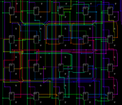
This example seems to be the vertical counter in the Lapis PCS bitstreams. There's a 10-bit counter going from DD to AF, and the logic in the middle seems to check for specific values to produce the VSYNC pulses and reset the counter when needed.
At this point I'm able to build proper nets from the interconnect data. I figured that giving them different colors would make it easier to tell them apart in the lack of better analysis solutions.
I'm looking at the bitstreams to try and see if I have any bugs, and I still do. For example, I just fixed a bug where the connection from AG.Y to BF.B and BG.B up there was missing. There are more -- for example I'm not seeing any clock input to the horizontal counter section, which is definitely odd.
A thing worth noting is that I do attempt to optimize nets by removing unused inputs. If you've looked at the XC2064 or XC2018 tools, you might have seen it was quite a mess. Technically, input muxes don't have a 'no input selected' setting, so there is always one input PIP active for each input. Additionally, production bitstreams will have all unused inputs tied together, which can create quite a mess. To get around this, I try to determine which inputs are relevant. For example, O and T inputs on IOBs will only be considered if the IOB is configured as an output, or tristate output, respectively. For CLBs we can just look at the LUTs, split them in two halves for a given input and see if these two halves are different.
Another example of a bug/oddity:
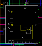
The CLB visual for one of the counter elements above. I'm not sure why the G equation is weird like that, A isn't even used as an input. The equation is supposed to be "G = (B ^ QY) * ~D". I think the equation code doesn't support XOR functions, but I'm not sure why it's pulling in A. Also, I might want to think of something regarding the length of the equation, because up there it doesn't fit the box.
All in all, it's coming together nicely I think. I'm thinking of eventually backporting it to the XC2064/18. Compared to the tracing code I had written in the XC2018 tool, this path system makes things so much easier to deal with.
Anyway, I'm mostly done with bitstream parsing and display. I'm working on tracing paths now.
(btw, the code is over at https://github.com/Arisotura/xc3000/tree/main if it's of any interest)
This is what we have:

This example seems to be the vertical counter in the Lapis PCS bitstreams. There's a 10-bit counter going from DD to AF, and the logic in the middle seems to check for specific values to produce the VSYNC pulses and reset the counter when needed.
At this point I'm able to build proper nets from the interconnect data. I figured that giving them different colors would make it easier to tell them apart in the lack of better analysis solutions.
I'm looking at the bitstreams to try and see if I have any bugs, and I still do. For example, I just fixed a bug where the connection from AG.Y to BF.B and BG.B up there was missing. There are more -- for example I'm not seeing any clock input to the horizontal counter section, which is definitely odd.
A thing worth noting is that I do attempt to optimize nets by removing unused inputs. If you've looked at the XC2064 or XC2018 tools, you might have seen it was quite a mess. Technically, input muxes don't have a 'no input selected' setting, so there is always one input PIP active for each input. Additionally, production bitstreams will have all unused inputs tied together, which can create quite a mess. To get around this, I try to determine which inputs are relevant. For example, O and T inputs on IOBs will only be considered if the IOB is configured as an output, or tristate output, respectively. For CLBs we can just look at the LUTs, split them in two halves for a given input and see if these two halves are different.
Another example of a bug/oddity:

The CLB visual for one of the counter elements above. I'm not sure why the G equation is weird like that, A isn't even used as an input. The equation is supposed to be "G = (B ^ QY) * ~D". I think the equation code doesn't support XOR functions, but I'm not sure why it's pulling in A. Also, I might want to think of something regarding the length of the equation, because up there it doesn't fit the box.
All in all, it's coming together nicely I think. I'm thinking of eventually backporting it to the XC2064/18. Compared to the tracing code I had written in the XC2018 tool, this path system makes things so much easier to deal with.
Arisotura
Well-known member
I couldn't resist, looked at the equations for the various counter checks in the first Lapis PCS bitstream (which outputs 640x480 60Hz).
The values I got out of it are as follows:
VBlank start: 480
VSync start: 483
VSync end: 486
VBlank end: 524
Visible area: 480 / Front porch: 3 / Sync pulse: 3 / Back porch: 38
HBlank start: 632
HSync start: 696
HSync end: 760
HBlank end: 888
Visible area: 632 / Front porch: 64 / Sync pulse: 64 / Back porch: 128
Compared to reference timings (http://www.tinyvga.com/vga-timing/640x480@60Hz), these are off, especially in the horizontal department. No wonder monitors don't like this video card.
I've also seen that the HSYNC output is HSync and VSync XORed together. I don't know how modern monitors like that.
-
Regarding the bitstream viewer thingy, a quick list of things that I still need to do:
* rework IOB clock lines, these don't work at the moment
* add tracing from tristate buffers and pull-ups (haven't seen any bitstream use them yet tho)
* a lot of cleanup
* maybe port my emulator thingy
I'm also thinking of adding features to ie. retrieve a netlist from the bitstream.
Similar threads
- Replies
- 70
- Views
- 4K
- Replies
- 4
- Views
- 532
- Replies
- 5
- Views
- 725
