cheesestraws
Well-known member
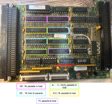
I was lucky enough to get hold of the Outbound Laptop docking card for the Macintosh SE. This card allows the Outbound Laptop to drive the zombified ROMless SE like a giant PDS card and use all its I/O. The card consists of a single programmable logic device and an enormous quantity of 74 series logic, nearly all of which are inverters and flipflops.
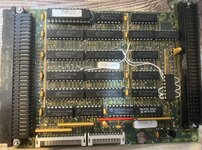
In this thread, I'm going to try to work out how it works, both for my own curiosity and also to reverse-engineer the pinout between it and the laptop, so I can use it. Stuff will get added to this thread as I have the energy and concentration to do it. Please do not expect speed.
Let's start with the data lines.
The treatment of each data line available on the SE PDS slot (D0..D15) is the same. Each data line has two latches, each with a three-state output. One latch has its output facing the data bus, one has its output away from it. Each of these latches attaches to a pin on JP2, the wider connector at the bottom of the photo above. This allows the Laptop to put 16 bits onto the bus by clocking a bit into one of the latches then enabling its output, or to temporarily latch a value off the bus by clocking a bit into the other latch, then when it is ready to have that bit appear on the pin on JP2, it can enable the output of that latch. A schematic for a single data line is thus:
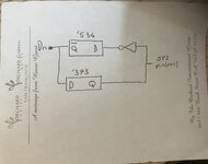
(the inverter is there because the output of the '534 is inverting, so the data needs to be inverted on the way in).
What about the address lines?
The address lines are similar, but unidirectional: the Laptop can set the address lines on the SE LB, but nothing on the SE LB can contorol the address bus as far as the Laptop is concerned. The address lines are multiplexed onto the same 16 pins on LP2. Observant readers will note that there are more than 16 address lines: there are two banks of address lines.
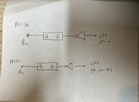
So, the laptop multiplexes all the address and data lines onto these 16 pins. How the latches are clocked and enabled is the next thing to work out, I think.

In this thread, I'm going to try to work out how it works, both for my own curiosity and also to reverse-engineer the pinout between it and the laptop, so I can use it. Stuff will get added to this thread as I have the energy and concentration to do it. Please do not expect speed.
Let's start with the data lines.
The treatment of each data line available on the SE PDS slot (D0..D15) is the same. Each data line has two latches, each with a three-state output. One latch has its output facing the data bus, one has its output away from it. Each of these latches attaches to a pin on JP2, the wider connector at the bottom of the photo above. This allows the Laptop to put 16 bits onto the bus by clocking a bit into one of the latches then enabling its output, or to temporarily latch a value off the bus by clocking a bit into the other latch, then when it is ready to have that bit appear on the pin on JP2, it can enable the output of that latch. A schematic for a single data line is thus:

(the inverter is there because the output of the '534 is inverting, so the data needs to be inverted on the way in).
What about the address lines?
The address lines are similar, but unidirectional: the Laptop can set the address lines on the SE LB, but nothing on the SE LB can contorol the address bus as far as the Laptop is concerned. The address lines are multiplexed onto the same 16 pins on LP2. Observant readers will note that there are more than 16 address lines: there are two banks of address lines.

So, the laptop multiplexes all the address and data lines onto these 16 pins. How the latches are clocked and enabled is the next thing to work out, I think.

