ZaneKaminski
Well-known member
I have designed the basic architecture for an accelerator “system” which can be adapted to any 68k Macintosh with a PDS slot.
The goals of the design were as follows:
I’ve designed the basic architecture implementing these features and have chosen all of the main (expensive) parts. What follows is my reasoning about the system and how I came to the conclusions which informed the design. Following that is the design I have thus far arrived at.
Originally, I looked for a 68k-compatible core which I could synthesize in an FPGA. Some cores exist which would give a nice boost to an SE, but were incompatible with ‘030 instructions, or I didn’t feel they would be fast enough. I had the feeling that a high-performance 68030-compatible soft core did exist, but could not realistically be licensed for this application. This approach would also be the cheapest way to implement the system, but I don’t know if it could be 50x faster than a Mac SE.
I am no CPU designer, nor do I intend to be; designing the core myself is not my interest. After a lot of thinking about it, I also concluded that the best 68k-compatible core built in an FPGA would be slower than the best 68k emulator running on a modern, cheap-ish microprocessor.
So I decided to pursue a solution where the 68k instructions are executed by emulator software running on an ARM microprocessor. Initially, I thought that the 68k instructions could be converted to ARM instructions in hardware, but this approach is, long story short, impossible given the details of the hardware available today and some details of the MC68k ISA, particularly the variable instruction size.
Instead, the 68k instructions would be translated to ARM in software. “Just-in-time compilation” is the term for this. I will explain more later. I already have a fairly detailed design for this part. Actually, the task of designing and implementing the emulator/translator is easier than the task of making the accelerator halfway affordable.
No existing emulator software is quite right for this purpose, and an OS would get in the way of achieving the highest performance. The goal is more of an emulator-kernel that runs without supervision.
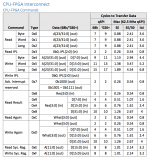
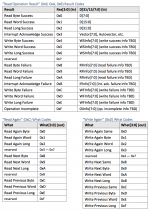
Along with the ARM processor, an FPGA would implement the bus interface (along with some level-shifters). The emulator would issue commands to the FPGA (e.g. read a longword from address 0x12345678), which would execute the operation on the PDS bus and then return the result to the emulator.
At this point, I was thinking that the accelerator would be too expensive to make. In particular, the requirements are a fast processor, high-bandwidth + low-latency CPU-FPGA interconnect, a cheap circuit board, and easy DIY assembly. These goals are all in competition!
Faster processor generally means more pins, so the PCB has to be more expensive. Same with having a higher-bandwidth interconnect. Both will require narrower traces and more layers. I accepted that the processor and RAM would come in a “BGA” package, which would be pretty hard to solder. So my aim was to keep the FPGA in a package that I can readily solder. I also wanted to avoid having a 6- or 8-layer board, which some would say is the minimum for a design of this complexity. That would be really expensive to make in small quantities.
The best option in terms of the FPGA-CPU interconnect would be to choose a CPU with a generic “external bus interface” to talk to the FPGA, along with a separate DDR2/3 controller. This would give the best throughput from the accelerator CPU to the Macintosh. (particularly the I/O devices, VRAM, ROM. We don’t need to touch main memory.) However, this would require more pins on the CPU (since it would have to have dual memory interfaces) and the FPGA. FPGAs with enough user I/O to do two wide bus interfaces are mostly BGA parts, which are hard to solder. A two-in-one FPGA+ARM SoC sounds good, since they have fast interconnects, but they are quite expensive and have a lot of pins, so that’s no good. Some high-speed serial interfaces (e.g. USB 2.0 high-speed) provide the requisite bandwidth, but their latency is too poor to do a good job with random-access. USB has as much throughput as an SE/30’s processor bus, but requires that data be transferred 512 bits at a time, when we really want to just transfer 32 bits of address, 32 bits of data, along with a 4- or 8-bit command. So in terms of latency, USB would be basically 8x slower than the PDS.
Complicating things further was a nagging detail about the implementation of the emulator. M68k has more registers than 32-bit ARM, so the entire state of the M68k (D0-7, A0-7, PC, etc.) cannot be entirely stored in the general-purpose registers of such an ARM processor. I would have to find some extra space in the ARM’s NEON registers or something. Maybe I could only store D0-D7 and the PC in the ARM general-purpose registers, and then I would have to stick A0-A7 in the NEON registers, moving address register values into the GP registers only when required. That sucks! Luckily, ARMv8-A “64-bit ARM” has plenty of registers, 31 x 64-bit. So an ARMv8-A chip would be nice. Just they are a bit rare outside of smartphones and usually have a lot of pins.
Additionally frustrating was the problem of adding video output. Ideally, the CPU would provide an RGB-type “LCD interface” that could be easily converted to VGA. But again, that requires more pins. The LCD interface could be part of the FPGA, but then the FPGA would have to have its own SDRAM or something, and the video performance would be constrained by the speed of the FPGA-CPU bus. Also then the FPGA would have to come in a BGA package because of pin count, which is undesirable.
So the aim was to pick a powerful processor with few pins, an FPGA with exposed pins (not BGA), and then get the cost for the board down somehow… All while ensuring that the FPGA-CPU interface is fast enough and that there’s enough bandwidth out of the CPU to an external peripheral board.
My solution was to divide the project into three separate boards:
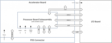
Note that I have indicated the specific interfaces between the processor board and the accelerator and I/O board. These interfaces will be discussed in greater detail later.
Three boards sounds expensive and difficult (three different products to make!), but the benefits are pretty clear:
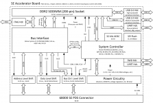
Okay, now let’s discuss my design for the main accelerator board. Here is one for a Macintosh SE.
The coolest and most expensive components (e.g. FPGA, processor) have already been chosen and their part numbers are marked in the image.
Other parts have not been explicitly chosen but I have provided a cost estimate for these parts.
“Dumb” parts like headers don’t have a cost estimate yet.
These diagrams only show the “main” component costs associated with the design. There will be lots of other little fiddly components that will cost money, but they are generally cheap.
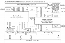
Here’s a similar diagram for the SE/30.
Since the SE/30 has wider address and data buses, the address and data lines coming from the FPGA are multiplexed to save pins on the FPGA. FPGAs with more pins than this one are either older and more expensive, or newer and in BGA package and still more expensive. Some will criticize the choice of an FPGA over a cheaper CPLD-type device, but $12 is cheap for an FPGA, and I am considering offloading part of the 68030 MMU emulation to the FPGA, justifying a more complex device. Actually, fully emulating the memory management unit is the bottleneck of 68030 emulation. We will have to see what the best way to do that is.
(Somewhat relevant are NeXT’s machines, which use a similar multiplexed address and data bus to communicate with their peripherals. Most of the Cube’s peripherals are accessed through special DMA-capable I/O ASICs, and so it’s basically free to build in to these custom chips a latch or two to demultiplex the bus. It saves room on the board.)
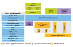
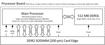
Here’s the processor board, showing my choice of processor, the NXP QorIQ LS1012A.
This processor is cheap for its speed ($20 in quantities of 10 or so), has the new “64-bit” ARMv8-A ISA, and has only 211 pins.
NXP says it’s designed for low-cost, 4-layer boards. That’s what we want. Actually, this processor is supposed to be for routers and network-attached storage, but it’s perfect for our application.
Also important to note is the minimum feature size of the processor board. 0.07mm is the minimum width for traces, less than half of the 0.15mm specified for the other boards. It would be too expensive to make the main board with such fine features.
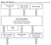
Here’s something pretty basic in the way of an I/O board. The idea is that the top edge of the graphic represents the ports facing out of the computer.
The microcontroller on here is from the Atmel SAM D21 family. It’s one of my favorites. It’s got a 48 MHz ARM Cortex-M0+ core. This is a really flexible chip that’s cheap. Especially cool is its clock system and generic clock generator peripheral. I used it for the system controller on the main board as well.
The features are WiFi, SD card slot, and a UART (serial port). Obviously these features will have to be implemented in the emulator software running on the processor.
By the way, XOSC is short for “crystal oscillator” and SWD is short for “single-wire debug,” used to program and debug ARM microcontrollers.
This board would have a USB connection through a header on the main board to the processor board. This is USB 2.0 “full speed,” meaning 12 Mbit/s. Too slow for video, but adequate for this SD card and serial stuff. 12 Mbit/s is slower than the SCSI on an SE/30, so that’s why I call this board “basic.”
Here’s a faster version of the same thing. Upgrading the processor to the Atmel SAM S70 series gives us some new interfaces and possibilities:
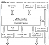
Here’s a quick sketch of a display board. I haven’t thought as much about this one.
USB 2.0 high-speed is just barely enough to do 8-bit 1024x768 x 60fps. 4-bit color would be more comfortable.
The basic idea is that the main processor can, during the vertical blanking interval, queue the entire frame to be sent over USB to the display controller. It can then figure out how to display it.
I don’t know how much a VGA DAC (digital-to-analog converter) costs.
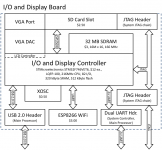
Higher resolutions and color depths are possible if a display controller with USB 3.0 is used. Right now, that's too expensive.
One of the problems with the entire design it is that the qSPI interface between the main processor and the bus interface FPGA puts a limit on the speed at which the accelerator can talk to the Mac’s RAM, VRAM (if any), ROM, and I/O devices. A 68000 bus access takes 4 cycles, and an ‘020+ access takes 3. It may take longer than that access for the processor to give an access command to the FPGA. The qSPI interface used for this is a 4-bit interface that can run at 62.5 MHz (limitation of the QorIQ LS1012A main processor).
Consider the case of writing to memory on a Macintosh SE, such as when changing the display. In order to write to memory, the main processor must transfer to the FPGA: a 4-bit command, 24-bit address, and 16-bit data. This takes 11 qSPI cycles at the 62.5 MHz, or 0.176 us. Then FPGA performs the bus access, taking 4 cycles (forget about waiting for the video circuitry access for a sec) at 7.83 MHz. So that’s 0.51 us. Then the processor must ask the FPGA what the result of the access was. That’s another 4 bit command and 4 bit data, at least. So 0.032 us. Therefore, the total time spent for the access is 0.72 microseconds, of which 0.21 us were wasted transferring data from the processor to the FPGA and vice-versa. That’s not that bad, representing a maximum PDS bus utilization of 71%.
But now consider the case of writing to VRAM on an SE/30. In order to write to memory, the main processor must transfer to the FPGA: a 4-bit command, 32-bit address, and 32-bit data. This takes 17 qSPI cycles at the 62.5 MHz, or 0.272 us. The bus access takes 3 cycles at 16.67 MHz: 0.18 us. Finally, 0.032 us is spend reading the result. Now, the total is 0.484 microseconds, of which only 0.18 us was spent using the PDS bus, for a utilization of 37%.
The case for a IIci is even worse, only 28% utilization. Also, the cycles may not line up perfectly, so I’ve given the best-case utilization here. As well, 8- and 16-bit reads and writes will give slightly better utilization percentages. For accesses that occur linearly in memory, “next address” and “previous address” commands can be implemented, saving the transfer of many address bits. That will improve it a little more. It may be possible for the emulator software to “pipeline" these memory operations, enqueuing another operation before the first is complete. Or maybe we can use two qSPI buses in parallel to realize a moderate increase in performance. I dunno.
This really only presents a problem for I/O. ROM is not a problem since it never changes and we just need to read it into the emulator’s memory once. RAM is not a problem since the emulator has its own RAM and we don’t need to mess with the Mac’s RAM except for the video portions. Video performance will be great, since instructions will never need to be fetched over the PDS bus and the video memory is usually written in linearly, so the accesses can be accelerated by the “next” and “previous” commands. The problem is I/O performance. I/O registers are not read or written linearly, and the I/O registers for the NCR 7530 SCSI chip, for example, are only 8 bits wide, which really bogs down the throughput. Indeed, users of IIci and faster Macintosh models may see slightly decreased SCSI and NuBus performance with this design. IWM and the other peripherals are not fast enough be negatively impacted. Of course, the rest of the system will be much faster, so it should be okay. You can turn on a huge disk cache and that will accelerate read operations.
So this problem with the qSPI kinda sucks but it’s not a big deal since every other aspect of the system is pretty fast.
Now, the big question: Does anyone actually want this? Each of the boards will probably cost $100 if they're produced in quantities of 25 or so each. The processor board might be a little more, the I/O boards, less. There are also a few hundred dollars of tooling fees that would have to be paid just once for the processor board in particular.
I can design the board for the SE, SE/30, and the processor board, and I can design the software for the main processor, system controller MCU, and also the FPGA bus interface. I will license my work under some kind of "open-source" license. I haven't decided which one I think is best yet. My hope is that, in releasing the design files for the accelerator board in particular, that I can inspire others in the community to adapt the board to other models of Macintosh beyond the SE and SE/30. I was gonna use KiCAD because it's free. Eagle's free versions are slightly not good enough for our purposes.
I am hoping someone else will design the I/O board(s) and their software. There are some mechanical problems to be solved there about how to mount the board in the hole of the SE and SE/30, and how to mount the SD card slot perpendicular to the board.
My next steps are:
The goals of the design were as follows:
- moderate cost
- at least 50x faster than Mac SE
- basic architecture can be used for any 68000, 68020, 68030 Mac with a PDS. Maybe 68040. (Especially SE, SE/30, IIci. IIfx difficult because of its unique I/O architecture.)
- maxes out the RAM of your system (probably can’t do this for IIfx and other DMA machines)
- enough bandwidth to connect peripherals: WiFi, SD card, display (at least 1024x768x4-bit)
I’ve designed the basic architecture implementing these features and have chosen all of the main (expensive) parts. What follows is my reasoning about the system and how I came to the conclusions which informed the design. Following that is the design I have thus far arrived at.
Originally, I looked for a 68k-compatible core which I could synthesize in an FPGA. Some cores exist which would give a nice boost to an SE, but were incompatible with ‘030 instructions, or I didn’t feel they would be fast enough. I had the feeling that a high-performance 68030-compatible soft core did exist, but could not realistically be licensed for this application. This approach would also be the cheapest way to implement the system, but I don’t know if it could be 50x faster than a Mac SE.
I am no CPU designer, nor do I intend to be; designing the core myself is not my interest. After a lot of thinking about it, I also concluded that the best 68k-compatible core built in an FPGA would be slower than the best 68k emulator running on a modern, cheap-ish microprocessor.
So I decided to pursue a solution where the 68k instructions are executed by emulator software running on an ARM microprocessor. Initially, I thought that the 68k instructions could be converted to ARM instructions in hardware, but this approach is, long story short, impossible given the details of the hardware available today and some details of the MC68k ISA, particularly the variable instruction size.
Instead, the 68k instructions would be translated to ARM in software. “Just-in-time compilation” is the term for this. I will explain more later. I already have a fairly detailed design for this part. Actually, the task of designing and implementing the emulator/translator is easier than the task of making the accelerator halfway affordable.
No existing emulator software is quite right for this purpose, and an OS would get in the way of achieving the highest performance. The goal is more of an emulator-kernel that runs without supervision.
Along with the ARM processor, an FPGA would implement the bus interface (along with some level-shifters). The emulator would issue commands to the FPGA (e.g. read a longword from address 0x12345678), which would execute the operation on the PDS bus and then return the result to the emulator.
At this point, I was thinking that the accelerator would be too expensive to make. In particular, the requirements are a fast processor, high-bandwidth + low-latency CPU-FPGA interconnect, a cheap circuit board, and easy DIY assembly. These goals are all in competition!
Faster processor generally means more pins, so the PCB has to be more expensive. Same with having a higher-bandwidth interconnect. Both will require narrower traces and more layers. I accepted that the processor and RAM would come in a “BGA” package, which would be pretty hard to solder. So my aim was to keep the FPGA in a package that I can readily solder. I also wanted to avoid having a 6- or 8-layer board, which some would say is the minimum for a design of this complexity. That would be really expensive to make in small quantities.
The best option in terms of the FPGA-CPU interconnect would be to choose a CPU with a generic “external bus interface” to talk to the FPGA, along with a separate DDR2/3 controller. This would give the best throughput from the accelerator CPU to the Macintosh. (particularly the I/O devices, VRAM, ROM. We don’t need to touch main memory.) However, this would require more pins on the CPU (since it would have to have dual memory interfaces) and the FPGA. FPGAs with enough user I/O to do two wide bus interfaces are mostly BGA parts, which are hard to solder. A two-in-one FPGA+ARM SoC sounds good, since they have fast interconnects, but they are quite expensive and have a lot of pins, so that’s no good. Some high-speed serial interfaces (e.g. USB 2.0 high-speed) provide the requisite bandwidth, but their latency is too poor to do a good job with random-access. USB has as much throughput as an SE/30’s processor bus, but requires that data be transferred 512 bits at a time, when we really want to just transfer 32 bits of address, 32 bits of data, along with a 4- or 8-bit command. So in terms of latency, USB would be basically 8x slower than the PDS.
Complicating things further was a nagging detail about the implementation of the emulator. M68k has more registers than 32-bit ARM, so the entire state of the M68k (D0-7, A0-7, PC, etc.) cannot be entirely stored in the general-purpose registers of such an ARM processor. I would have to find some extra space in the ARM’s NEON registers or something. Maybe I could only store D0-D7 and the PC in the ARM general-purpose registers, and then I would have to stick A0-A7 in the NEON registers, moving address register values into the GP registers only when required. That sucks! Luckily, ARMv8-A “64-bit ARM” has plenty of registers, 31 x 64-bit. So an ARMv8-A chip would be nice. Just they are a bit rare outside of smartphones and usually have a lot of pins.
Additionally frustrating was the problem of adding video output. Ideally, the CPU would provide an RGB-type “LCD interface” that could be easily converted to VGA. But again, that requires more pins. The LCD interface could be part of the FPGA, but then the FPGA would have to have its own SDRAM or something, and the video performance would be constrained by the speed of the FPGA-CPU bus. Also then the FPGA would have to come in a BGA package because of pin count, which is undesirable.
So the aim was to pick a powerful processor with few pins, an FPGA with exposed pins (not BGA), and then get the cost for the board down somehow… All while ensuring that the FPGA-CPU interface is fast enough and that there’s enough bandwidth out of the CPU to an external peripheral board.
My solution was to divide the project into three separate boards:
- Main accelerator board, which will plug into the Mac. This will be different for each machine supported.
- Processor system-on-a-module card, shaped like a DDR2 SODIMM, but containing just the processor and its RAM. This will plug into the accelerator board.
- I/O board, optional. Connects to the processor card via USB through the main accelerator board. This would go in the hole on the back of the Mac SE or would be a dummy NuBus card. (NuBus is slow, no need to actually use it.)

Note that I have indicated the specific interfaces between the processor board and the accelerator and I/O board. These interfaces will be discussed in greater detail later.
Three boards sounds expensive and difficult (three different products to make!), but the benefits are pretty clear:
- The same processor card can fit into accelerators for different machines.
- In the future, someone else can make a faster processor card that plugs into the existing main board. I have defined a minimum set of I/O interfaces that the processor card must support. Almost all modern MPUs have these interfaces, so the design of the processor card is quite orthogonal to the design of the main board.
- Vice-versa, too. Same processor card can plug into an improved main board.
- Encourages future development of peripheral I/O hardware, since the I/O board is separate and will be much easier to design than the other two pieces. Someone can add video output that way.
- The processor card has to be very dense, and a dense PCB costs more. If the entire board had to have the density of the processor card, it would be prohibitively expensive.
- Since the processor card is relatively simple, hopefully I will get it right the first time. The other parts will be cheaper to redo if I mess up on them.
- I can definitely assemble the main board and I/O boards myself. The processor board has these BGA parts that most consider to be impossible to DIY solder. It certainly is possible, just difficult. I prefer using a hot plate to solder SMD components, but I’ve never done BGA. Professional assembly and testing is expensive in small quantities, so we want to minimize the size and amount of parts on the processor board in case we have to go that route.
Okay, now let’s discuss my design for the main accelerator board. Here is one for a Macintosh SE.
The coolest and most expensive components (e.g. FPGA, processor) have already been chosen and their part numbers are marked in the image.
Other parts have not been explicitly chosen but I have provided a cost estimate for these parts.
“Dumb” parts like headers don’t have a cost estimate yet.
These diagrams only show the “main” component costs associated with the design. There will be lots of other little fiddly components that will cost money, but they are generally cheap.

Here’s a similar diagram for the SE/30.
Since the SE/30 has wider address and data buses, the address and data lines coming from the FPGA are multiplexed to save pins on the FPGA. FPGAs with more pins than this one are either older and more expensive, or newer and in BGA package and still more expensive. Some will criticize the choice of an FPGA over a cheaper CPLD-type device, but $12 is cheap for an FPGA, and I am considering offloading part of the 68030 MMU emulation to the FPGA, justifying a more complex device. Actually, fully emulating the memory management unit is the bottleneck of 68030 emulation. We will have to see what the best way to do that is.
(Somewhat relevant are NeXT’s machines, which use a similar multiplexed address and data bus to communicate with their peripherals. Most of the Cube’s peripherals are accessed through special DMA-capable I/O ASICs, and so it’s basically free to build in to these custom chips a latch or two to demultiplex the bus. It saves room on the board.)

Here’s the processor board, showing my choice of processor, the NXP QorIQ LS1012A.
This processor is cheap for its speed ($20 in quantities of 10 or so), has the new “64-bit” ARMv8-A ISA, and has only 211 pins.
NXP says it’s designed for low-cost, 4-layer boards. That’s what we want. Actually, this processor is supposed to be for routers and network-attached storage, but it’s perfect for our application.
Also important to note is the minimum feature size of the processor board. 0.07mm is the minimum width for traces, less than half of the 0.15mm specified for the other boards. It would be too expensive to make the main board with such fine features.

Here’s something pretty basic in the way of an I/O board. The idea is that the top edge of the graphic represents the ports facing out of the computer.
The microcontroller on here is from the Atmel SAM D21 family. It’s one of my favorites. It’s got a 48 MHz ARM Cortex-M0+ core. This is a really flexible chip that’s cheap. Especially cool is its clock system and generic clock generator peripheral. I used it for the system controller on the main board as well.
The features are WiFi, SD card slot, and a UART (serial port). Obviously these features will have to be implemented in the emulator software running on the processor.
By the way, XOSC is short for “crystal oscillator” and SWD is short for “single-wire debug,” used to program and debug ARM microcontrollers.
This board would have a USB connection through a header on the main board to the processor board. This is USB 2.0 “full speed,” meaning 12 Mbit/s. Too slow for video, but adequate for this SD card and serial stuff. 12 Mbit/s is slower than the SCSI on an SE/30, so that’s why I call this board “basic.”

Here’s a faster version of the same thing. Upgrading the processor to the Atmel SAM S70 series gives us some new interfaces and possibilities:
- USB 2.0 “high-speed” satisfies fully any desire for SD card and WiFi performance. 480 Mbit/sec blows away the I/O on even the original iMac. (It used only “full speed”)
- This microcontroller supports JTAG, which allows us to use a single port to program and debug the I/O controller, bus interface FPGA, and the main processor. Convenient.
- Also the processor is like 8x faster than the I/O controller on the slower board. Sounds like overkill, but this is the cheapest microcontroller with high-speed USB 2.0.

Here’s a quick sketch of a display board. I haven’t thought as much about this one.
USB 2.0 high-speed is just barely enough to do 8-bit 1024x768 x 60fps. 4-bit color would be more comfortable.
The basic idea is that the main processor can, during the vertical blanking interval, queue the entire frame to be sent over USB to the display controller. It can then figure out how to display it.
I don’t know how much a VGA DAC (digital-to-analog converter) costs.

Higher resolutions and color depths are possible if a display controller with USB 3.0 is used. Right now, that's too expensive.
One of the problems with the entire design it is that the qSPI interface between the main processor and the bus interface FPGA puts a limit on the speed at which the accelerator can talk to the Mac’s RAM, VRAM (if any), ROM, and I/O devices. A 68000 bus access takes 4 cycles, and an ‘020+ access takes 3. It may take longer than that access for the processor to give an access command to the FPGA. The qSPI interface used for this is a 4-bit interface that can run at 62.5 MHz (limitation of the QorIQ LS1012A main processor).
Consider the case of writing to memory on a Macintosh SE, such as when changing the display. In order to write to memory, the main processor must transfer to the FPGA: a 4-bit command, 24-bit address, and 16-bit data. This takes 11 qSPI cycles at the 62.5 MHz, or 0.176 us. Then FPGA performs the bus access, taking 4 cycles (forget about waiting for the video circuitry access for a sec) at 7.83 MHz. So that’s 0.51 us. Then the processor must ask the FPGA what the result of the access was. That’s another 4 bit command and 4 bit data, at least. So 0.032 us. Therefore, the total time spent for the access is 0.72 microseconds, of which 0.21 us were wasted transferring data from the processor to the FPGA and vice-versa. That’s not that bad, representing a maximum PDS bus utilization of 71%.
But now consider the case of writing to VRAM on an SE/30. In order to write to memory, the main processor must transfer to the FPGA: a 4-bit command, 32-bit address, and 32-bit data. This takes 17 qSPI cycles at the 62.5 MHz, or 0.272 us. The bus access takes 3 cycles at 16.67 MHz: 0.18 us. Finally, 0.032 us is spend reading the result. Now, the total is 0.484 microseconds, of which only 0.18 us was spent using the PDS bus, for a utilization of 37%.
The case for a IIci is even worse, only 28% utilization. Also, the cycles may not line up perfectly, so I’ve given the best-case utilization here. As well, 8- and 16-bit reads and writes will give slightly better utilization percentages. For accesses that occur linearly in memory, “next address” and “previous address” commands can be implemented, saving the transfer of many address bits. That will improve it a little more. It may be possible for the emulator software to “pipeline" these memory operations, enqueuing another operation before the first is complete. Or maybe we can use two qSPI buses in parallel to realize a moderate increase in performance. I dunno.
This really only presents a problem for I/O. ROM is not a problem since it never changes and we just need to read it into the emulator’s memory once. RAM is not a problem since the emulator has its own RAM and we don’t need to mess with the Mac’s RAM except for the video portions. Video performance will be great, since instructions will never need to be fetched over the PDS bus and the video memory is usually written in linearly, so the accesses can be accelerated by the “next” and “previous” commands. The problem is I/O performance. I/O registers are not read or written linearly, and the I/O registers for the NCR 7530 SCSI chip, for example, are only 8 bits wide, which really bogs down the throughput. Indeed, users of IIci and faster Macintosh models may see slightly decreased SCSI and NuBus performance with this design. IWM and the other peripherals are not fast enough be negatively impacted. Of course, the rest of the system will be much faster, so it should be okay. You can turn on a huge disk cache and that will accelerate read operations.
So this problem with the qSPI kinda sucks but it’s not a big deal since every other aspect of the system is pretty fast.
Now, the big question: Does anyone actually want this? Each of the boards will probably cost $100 if they're produced in quantities of 25 or so each. The processor board might be a little more, the I/O boards, less. There are also a few hundred dollars of tooling fees that would have to be paid just once for the processor board in particular.
I can design the board for the SE, SE/30, and the processor board, and I can design the software for the main processor, system controller MCU, and also the FPGA bus interface. I will license my work under some kind of "open-source" license. I haven't decided which one I think is best yet. My hope is that, in releasing the design files for the accelerator board in particular, that I can inspire others in the community to adapt the board to other models of Macintosh beyond the SE and SE/30. I was gonna use KiCAD because it's free. Eagle's free versions are slightly not good enough for our purposes.
I am hoping someone else will design the I/O board(s) and their software. There are some mechanical problems to be solved there about how to mount the board in the hole of the SE and SE/30, and how to mount the SD card slot perpendicular to the board.
My next steps are:
- Obtain full manual (probably 3000 pages) for the NXP QorIQ LS1012A processor (this information is "embargoed" and so I must sign an NDA to receive it)
- Create schematic symbols and footprints for all components
- Create the basic board shapes for the SE and SE/30 main boards, and the processor board (to get a better idea of the required PCB size and cost)
- Start designing schematics for one of the accelerator boards (SE or SE/30) and the processor board (according to the block diagrams given in this post)
Last edited by a moderator:

