• Updated 2023-07-12: Hello, Guest! Welcome back, and be sure to check out this follow-up post about our outage a week or so ago.

Serious proposal: accelerator and peripheral expansion system

ZaneKaminski

Well-known member
I've decided that the FPGA isn't really necessary if we bit-bang the signals out via a wide GPIO port. That should be faster since the data doesn't need to first be transferred over a slow connection from the processor to the FPGA. Since these processors in question run at basically GHz speeds, they are certainly fast enough to bit-bang the 68000 and '020/'030 buses.

The only problem is that the QorIQ LS1012A doesn't have enough pins to talk directly to the PDS, even if we muliplex address and data. There are some faster members of the QorIQ family, but they're basically non-options because of their steep price. The only reason I'm looking at the LS1012A is how cheap it is to integrate into a system.

Qualcomm has started selling their Snapdragon 410E through resellers, which is a very capable chip (4 x 1.2 GHz Cortex-A53). The chip itself is only $18 or so, less than the QorIQ, but it will be difficult and expensive to integrate into a board. I think much of the hardware information about this chip is "secret" as well, so that may make it difficult to develop "bare-on-the-metal" software for it.

There are some Snapdragon 410E "system-on-a-module" units for sale, but they don't break out enough consecutively-numbered GPIO pins to make it worth using without the FPGA. We want something that outputs, for example, GPIO 0-31, so we can hook those up to the adddress or data bus or whatever of the Mac. If, for example GPIO16 were to be missing, then we will have to spend some CPU cycles rearranging the data before we put it on the bus. The Snapdragon 410E pre-built modules available were not necessarily designed with this requirement in mind.

On the upside, the Snapdragon 410E is way fast, and multiple cores can allow us to parallelize translation of the Mac opcodes and some of the MMU housekeeping so as to make the system even faster.

Also, the DragonBoard 410c, a $75 development board integrating the Snapdragon 410E, is available, and it's got USB and an HDMI port. Combined with a little Mac peripheral emulation software (for the VIA, IWM, display, etc.), that takes us very close to a super-Macintosh on a board for $75. Just add monitor, keyboard, and mouse. The primary difficulty in adapting an emulator to standalone operation on the DragonBoard is the lack of documentation on the USB and HDMI stuff of the 410E.

Also the 410E can run Android hahahah.

Again, the major problem with all this is that the processor board with the 410E will cost a lot more than the one for the QorIQ. Even if we eliminate the FPGA and shrink the main board as small as we can, the Snapdragon will still mean greater cost and difficulty. If I get far with the Snapdragon, I'll launch a kickstarter for the processor board. It should be useful for many other applications. If a lot of people want the processor board (for use in the "Maccelerator" or otherwise), then the unit cost will be lower.

I think I will try both the QorIQ and the Snapdragon. Still haven't received the QorIQ datasheet from the sales rep. Hopefully it'll arrive soon.


techknight

Well-known member
I wonder though if you could use the AM335X chips? Because at least you have a couple PRUs available for play with the bus while you still have the main ARM core available for whatever usage. 


ZaneKaminski

Well-known member
Well, the problem with those chips is that they're ARMv7-A. We could use them, but I have a preference for ARMv8-A since it has 31 general-purpose registers to ARMv7-A's 15. That's convenient because M68k has 16 registers, so on ARMv8-A, we can fit D0-D7, A0-A7, PC, status register stuff (X bit will be tricky), and still have room for scratch registers. Without as many registers, an ARMv7-A implementation will have to swap the stored M68k registers out to memory or something. That will slow things down.

However, I acknowledge that my preference for ARMv8-A could be driving up the system cost. I will look into the possibility of storing the 16 M68k general-purpose registers in ARMv7-A's NEON registers.

Those AM335x chips have around the pin count I'm looking for though. The Snapdragon 410E has 760 balls at 0.4" pitch, compares to 211 for the QorIQ. Qualcomm says you need at least two, but preferably four types of microvias to route all of the signals. Ugh. That's expensive. I'm trying to get the full pinout and footprint for the Snapdragon, and then I'll see how hard it will be to do the board.

Something around 300-400 BGA balls sounds like it'll have the right amount of I/O but still be easy to break out the signals.


ZaneKaminski

Well-known member
The PRU-ICSS system in those TI chips is really cool though. I just figured that I could do the bus communication on the main processor, but the timing predictability of the PRU system is attractive.

I figured the strategy of performing a bus access on the main ARM chip would be to poll the clock, dtack, etc., and once we observe the right edge on the right signal, drive the data we want on the bus, take it off, whatever. If the goal is to support a IIci, however, I've never bit-banged at 25 MHz. So we've gotta make sure that'll actually work. I'm concerned that, at 25 MHz, there may be a big delay between when an edge occurs and when the GPIO system of the processor recognizes that edge.

It would be much nicer to clock the chip at a multiple of the Mac's clock and in phase with it, and write code to with exact timing to access the bus. Then we would never have to poll the clock. That's not gonna happen on one of these big fancy ARM microprocessors. Some ARM microcontrollers have a mode that makes instruction timing completely predictable, but setting that mode negates all of the benefits of the cache and and branch prediction and all that.

I've gotta examine the timing margins for the M68k family buses (especially the synchronous accesses, since they are gonna be tighter and obviously will have a defined relationship with the clock), and then I'll look at how long input and output signals take to propagate in these GPIO systems.

In the AM335x, the fact that the PRUs are separate from the ARM CPU seems good, but I can't think of a purpose of parallelizing the execution of translated instructions with accessing the bus. There's no point unless we decide to "pipeline" the operations in the software, speculatively execuing future code while a bus access is pending. Pipelining works great in hardware, but in software, it would probably be a mess and slow things down more than it would help. Maybe while the PRU is busy accessing the bus, the main processor can do housekeeping functions or speculatively translate more code.

 
Last edited by a moderator:

ZaneKaminski

Well-known member
TI AM437x may also be a good choice. Only $20 for a 1 GHz one with a Cortex-A9 and four PRU cores. I understand the Cortex-A9 in these chips to be a good bit faster than the Cortex-A8 in the AM335x series.

There's also NXP's i.MX6 series, which goes down to around $30 for 2x ARM Cortex-A9 at 1GHz or so. No fancy PRU though.

i.MX7 has more of a low-power focus... no reason to spend money on that when we could be spending money on making the system faster. The older i.MX chips are basically irrelevant. i.MX8 is coming as well, but I think those chips will only support DDR4 memory, which is sort of a bummer. DDR4 is so distant from the "makerspace" that having it in the design would certainly make it impossible to produce for a reasonable price.


ZaneKaminski

Well-known member
I have reworked my design. The major changes are:

- Processor board (Snapdragon 410E) sourced externally, not designed by me
- FPGA has been eliminated
- No USB 3.0
- Has microSD slot on accelerator board
- Small CPLD implements interrupt priority control
 
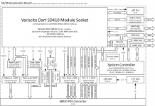
Here are the block diagram pictures for SE and SE/30. There is a lot more detail about the bus signals now... I've figured that aspect out pretty fully.
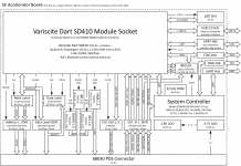
68000Board.png
68030Board.png
 
The benefits are lower cost, faster processing, and less special software that must be written.
 
I decided to go with the Snapdragon 410E, but it was impossible for me to get on a board at a reasonable price. Luckily, Variscite sells the Dart SD410 module, which has the 410E, associated power management IC, 1 GByte LPDDR3, 8 GBytes eMMC flash, ad WiFi, Bluetooth, GPS, FM radio capability (external antenna needed).
 
The SD410 module will be mounted on the board with two connectors that are about $1.50 each. It’s also half the size of a DDR2 SODIMM.
 
I’ve eliminated the FPGA and now am using the SD410’s GPIO and some latches and level-shifters to implement the bus interface.
 
Since the FPGA was supposed to be a QFP-type part, not BGA, this and the smaller processor module will allow us to greatly reduce the size of the main board.
 
I think that the Snapdragon can run a custom-rolled version of Linux. The details of the Snapdragon 410E are so complicated, secret, and proprietary, that if we ran our code bare-on-the-metal or rolled our own RTOS, we would be missing out on so many capabilities and the benefits of fully-developed driver software.
 
The WiFi and Bluetooth functionality on the SD410 module are two obvious things we’d be missing without using Linux. However, the use of Linux will allow individuals who are more experienced in Linux system administration, rather than system design, programming, EE, etc., to contribute and make the Maccelerator better.
 
Now, in order to run Linux, the accelerator process which actually executes the code must run as some kind of a driver so that it can directly manipulate the GPIO pin control I/O registers without needing to perform a context switch. Either that or the emulator can run in userspace and just the bus stuff can run as a driver. That’s the correct way to do it, but I’m trying to achieve the best performance possible with the amount of time and money I can devote to the project. We will see.
 
Since we’re running Linux, there is less of a need for the I/O board, especially if we can get the SD410’s WiFi and Bluetooth working. The I/O board also is a bit mechanically difficult, in terms of the amount of room available for it. Rather than the I/O board, a much cheaper option would be to just run USB to the back of the Mac. Nonetheless, I/O boards will still be supported.
 
Anyway, here’s a rough bil of materials (for SE/30):
Variscite Dart SD410 (Processor Board)     1 x $57   = $57
Hirose DF40C-90DS-0.4V (SD410 conn.)       2 x $1.50 = $3
Euro-DIN 120 (PDS Connector)               1 x $7.50 = $7.50
Atmel SAMD10D14 (System Controller)        1 x $2    = $2
Lattice LC4032ZE (IRQ Controller)          1 x $1    = $1
microSD slot                               est.      = $2.50
16-bit latch                               4 x $0.50 = $2
16-bit level shift                         6 x $1.50 = $9
1-bit level shift                          3 x $0.50 = $1.50
32.768 kHz crystal oscillator              1 x $0.50 = $0.50
Power stuff (L, bypass C, V. regs.)        est.      = $5
PCB                                        est.      = $15
 
This stuff totals $106. This is without a doubt an underestimate of the final cost (assembly, shipping, packaging, etc. not included), but we should be able to it out the door for under $150, as long as 15 or so people want one. I will work on making it even cheaper.
 
Last edited by a moderator:

ZaneKaminski

Well-known member
I've been looking into how to convert the Snapdragon's MIPI-DSI display interface into something supported by modern monitors.

Unfortunately, there does not seem to be an easy solution. Few ICs exist which convert DSI to anything useful, and the ones that do are usually very small BGA-type parts, being targeted at smartphone and other similar applications.

I will break out the MIPI-DSI interface and maybe someone else will be able to solve the problem. It would be cool to see a Micron Xceed-type grayscale mod running from the DSI interface!

So for now we will still have to run video over the USB 2.0 link to an I/O board. That presents some bandwidth constraints but it should work okay.

The Snapdragon 410 also has dual MIPI-CSI camera interfaces. I don't think I'm gonna expose connectors on the accelerator card for those. No need.

 
Last edited by a moderator:

Bunsen

Admin-Witchfinder-General
I'm astonished.  And very interested.

Just out of curiosity, what led you to choose the Snapdragon over this one you mentioned earlier?

TI AM437x / $20 for a 1 GHz one with a Cortex-A9 and four PRU cores.
I'm also sending you a PM now.  Check your MLA mailbox at the top of the page ;)


Bunsen

Admin-Witchfinder-General
And while I realise it's a somewhat less grunty processor than the one you're looking at, I'll just drop in the BeagleBone Black here as a suggestion.  It's a ready-built board for US$55 in small quantities, with a 1GHz AM335x A8, two 200MHz PRUs (92 pins on DIL headers), 512MB of DDR3, SD and eMMC, USB client and host, Ethernet, and HDMI out.

It's also an open-hardware design which could be forked if necessary, say for a faster ARM.

 
Last edited by a moderator:

Bunsen

Admin-Witchfinder-General
So for now we will still have to run video over the USB 2.0 link to an I/O board. That presents some bandwidth constraints but it should work okay.
USB video out converters (VGA, HDMI, DVI) are available retail.  If you're running a *nix on your board, those would be an option.


ZaneKaminski

Well-known member
Well, the Snapdragon 410 is quite fast compared to basically anything else at anywhere close of a price-point. I was stupid to try and get it on a board myself... the tooling costs alone would be $1200+, and then as much as $100 for each PCB. So the Variscite SD410 module seemed to be the solution. Variscite's website says it "starts at $57." I don't know if that means you have to buy 1000 or something to get it for $57, or if they'll sell you 1 or 10 or something at that unit price. I tried to get a quote but they haven't responded. I'll try and call them later today.

As for the TI chips, the PRU system I looked at on the AM335x and AM437x didn't seem to have enough I/O pins per PRU core to accommodate operation with the PDS bus. I think on the AM437x, they only had 20 pins per core, and there are already 30 or so control signals (for the level shifter control and for the M68k bus) that have to be manipulated. I wasn't sure if I could parallelize the operation across multiple PRU cores, which would give 20 extra pins per core. The Snapdragon 410, which has as many as 122 I/O pins, was a better choice in my mind.

The disadvantage of the Snapdragon is that we have to run Linux or Windows CE or something or else; with little documentation from Qualcomm, we'll miss out on any cool features of the hardware.

The main issue with running Linux is ensuring that the bus driver can directly manipulate the GPIO pin registers in memory, and can do so without being preempted, for as long as a microsecond or so (~length of bus cycle). With a single-core processor, I would say this approach sucks, but with four cores, hogging one to operate the bus sounds fine. Once I make more progress on the schematic (which is coming along), I will purchase the DragonBoard 410c evaluation kit and learn more about building a custom Linux distro for the Maccelerator.

So yeah, the BeagleBone could work, but as long as the SD410 module is cheap enough, I think it's a better choice.

The only functionality the BeagleBone offers that would be hard to get with the SD410 module is HDMI. All of the chips to convert DSI to HDMI or anything else useful are just too small to implement cheaply in the design. The USB video converters must have a driver that compresses the video, then the adapter must decode it before sending it to the screen. Hopefully we can support that without too much effort. I'm gonna put a single USB Type-A port on the accelerator card, and then either a generic hub, video adapter, whatever, can be plugged into it, or a custom module designed to fit the SE and SE/30.

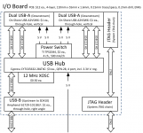
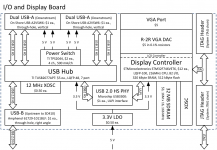
By the way, here are my sketches of USB hub and hub+video cards for the SE and SE/30. I dunno if these would be in too much demand, given that they aren't really supposed to be used independently of the accelerator.

Peripheral Connector.png

Video Connector.png

The idea of how to structure the software for four cores is as follows:

Put the bus operation and the emulation function in the same thread, running like a driver, as part of the kernel. That way, context switches will be avoided when performing a bus access. The other three cores will run the OS normally.

The emulator should be able to either run a cached translation of some M68k code, or, if no translation is available, queue that block of code for translation and then interpret it. In performing interpretation as well as translation, we get the great performance of translation, but the option to interpret ensures that there will never be a long delay in results that would cause, for example, a floppy operation to go awry. The translation can be performed on a different core than the emulator and bus stuff. It would just have to some share memory with the driver process. Dunno how to do that, but I'm sure it's all possible. 


ZaneKaminski

Well-known member
I've made a lot of progress on the accelerator card schematic for the Mac SE. I'm attaching what I have so far as a PDF. I'll release the KiCAD .sch files when I feel it's finished. There are some problems, oversights, areas of sloppiness, etc. in the current schematic.

Maccelerator-SE.pdf

In particular, I need to add some more power filtering and bypass stuff, switch to a system controller with more I/O, make sure I have series protection resistors in the right areas for the address-data and IRQ bidirectional buses, add pull-ups resistors and filtering to the SD410's reset pins for good measure, add a way for the for the system controller to reset the SD410 system-on-a-module without powering it down and back up, uhh, that's all I can think of right now.

Once I'm done with the SE, I'll port what I have for the SE to the SE/30, and then I'll begin the board designs.


Attachments

  • Maccelerator-SE.pdf
    1.3 MB · Views: 206
Last edited by a moderator:

ZaneKaminski

Well-known member
In addition to the Variscite Dart SD410 module:

http://www.variscite.com/products/system-on-module-som/cortex-a53-krait/dart-sd410-qualcomm-snapdragon-410

There are also these options:

http://www.inforcecomputing.com/products/system-on-modules-som/qualcomm-snapdragon-410-inforce-6301-micro-som

http://shop.intrinsyc.com/products/open-q-410-system-on-module

https://eragon.einfochips.com/products/system-on-modules/eic-q410-200.html

It turns out that Variscite does not sell single units of their SD410 module. Either we have to buy a lot, find a distributor that sells them, or change the specific system-on-a-module used. The other three manufacturers of similar Snapdragon 410 modules I linked do sell singles, but I'm not sure that the other three modules expose the right amount of I/O for our purposes. I will investigate further.


ZaneKaminski

Well-known member
I finished fixing most of the problems in the schematic I mentioned yesterday, but now a new issue has come to my attention.

Something like 46 pins are required to operate the 68000 bus and 53 are required for 68030. Plus there are 6 (4 and 2) signals for two UARTs. I am gonna more heavily multiplex some of the functions. Many of the available Snapdragon 410 SoMs just don't break out enough GPIO pins.

I will redesign the bus interface to be more heavily multiplexed. The current design has a 16-bit bus shared for address and data. I think I'm gonna change it to an 8-bit bus multiplexed between address, data, IPL, and FC.

That will require another CPLD or two to implement. They're only a buck or so.

Edit: I've figured something out which will should only take 29 pins in the case of 68030, and 24 for 68000. The disadvantage of this approach is that it uses an 8-bit bus multiplexed 15 times over... So some microseconds will wasted as all of the 15 latches are loaded with data.

Not sure if anyone will be able to make sense of it, but here is my sketch of what signals are required for this scheme:

(8 ) B[07:00] multiplexed over the following functions:

  • Aout[07:00] output to A latch
  • Aout[15:08] output to A latch
  • Aout[23:16] output to A latch
  • Aout[31:24] output to A latch
  • Dout[07:00] output to D latch
  • Dout[15:08] output to D latch
  • Dout[23:16] output to D latch
  • Dout[31:24] output to D latch
  • Din[07:00] input from D latch
  • Din[15:08] input from D latch
  • Din[23:16] input from D latch
  • Din[31:24] input from D latch
  • BusCtrlOut[7:0]
  • [ FC[2:0], IPLset[2:0], 0b00 } output to FC latch, output to IPL priority
  • IPLin[2:0] current IPL input
 
(1) BOLE bus output/latch enable
(3) Bsel[3:0] chooses which signals to output on bus
 
(1) ALSOE enables output of A[31:0] during read and write cycles
(1) DLSOE enables output of D[31:0] during write cycle
(1) DinLE latches input D[31:0] during read cycle
(1) CLSOE enables output of other bus control signals
 
(1) BG (in) 
(3) HALT, BERR, RESET
(1) REQ_RESET
 
BusCtrlOut[7:0] for 68000
  • LDS (out)
  • UDS (out)
  • VMA (out)
  • RW (out)
  • AS (out)
  • BR (out)
  • BGACK (out)
 
BusCtrlOut[7:0] for 68030
  • SIZ[1:0] (out)
  • CIOUT (out)
  • CBREQ (out)
  • RW (out)
  • AS (out)
  • BR (out)
  • BGACK (out)
 
68000 only: (3)
  • (1) DTACK (in)
  • (1) VPA (in)
  • (1) PMCYC (in)
 
68030 only: (8 )
(1) PWROFF (in)
(2) DSACK[1:0] (in)
(2) STERM (in), CBACK (in)
(3) DOrder[2:0] (out) chooses what data order to choose (for 68030 dynamic bus sizing)
  • 000: normal
  • 001: 2nd 8-bit word
  • 010: 3rd 8-bit word
  • 011: 4th 8-bit word
  • 100: 2nd 16-bit transfer
 
Last edited by a moderator:

sstaylor

Well-known member
I don't know anything about digital electronics but I've gotta say I'm fascinated reading through your updates and excited about your project.  Keep up the good work!


ZaneKaminski

Well-known member
Thank you for the encouraging words, sstaylor.

I've abandoned the idea of using the processor itself to do the timing-intensive work for interfacing with the bus. Instead, I've implemented a design where 3 very cheap FPGAs implement the bus logic. The FPGAs are from Lattice's MachXO series and are about $2.50 each. This approach is much less costly than the original design with the Altera Cyclone IV FPGA implementing the bus interface, but still costs more than the schematic I posted last week. These cheap little MachXO chips have many cost and board size advantages over a more complex unit like the Cyclone IV.

The interface between the FPGA and Snapdragon is also going to be fully asynchronous now, meaning that the Snapdragon does not need to implement any precise timing to talk to the bus FPGAs.

I've also cleaned up the schematic in the ways I've wanted, for example adding more electrostatic discharge protection, upgrading the system controller, etc. I will post another schematic for Mac SE later today, and then I'll port it to SE/30.

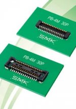
The coolest feature I've added in this version is certainly the display sub-board connector. I've added a low-profile, shielded, 30-pin board-to-board connector that breaks out the MIPI-DSI display interface. Looks like this:

Featured_P2_pb4m2014-2.jpg

Additionally, I've found that an FPGA from the Lattice MachXO3 series is probably the cheapest way to convert the high-speed DSI to a more workable digital or analog signal, for example to implement VGA or a Micron Xceed-style grayscale solution for the SE/30. The path I'm seeing to achieving grayscale is to clone the Xceed yoke board (hopefully they won't mind lol), figure out what inputs it accepts, and then design a display sub-board to generate that from the DSI interface.

Okay, now the bad news is that the Variscite Dart SD410 module can't be purchased for $57 as advertised, and so I have switched to the Intrinsyc Open-Q 410 module (https://www.intrinsyc.com/computing-platforms/410-som/), which can be purchased in single quantities for $79. The switch to the MachXO FPGAs were a consequence of this change, since the Intrinsyc module has fewer I/O pins than the Variscite one. Should work better this way, anyway, though the FPGAs have increased the cost by another few dollars.

 
Last edited by a moderator:

ZaneKaminski

Well-known member
Here's another nagging detail about the grayscale output on SE/30.

Note the bandwidth requirement for 8-bit grayscale on a compact Mac.

512 x 342 x 60.15fps x 8bit = 84 Mbit/sec
 
84 Mbit/sec is very manageable over USB, so maybe the grayscale output should be a feature of the I/O board for the SE and SE/30. That makes sense because those USB hub I/O boards I posted the block diagram for a week ago will only fit in compact Macs. That would be a cool feature that would make the I/O board more enticing.
 
But then the I/O board can't have VGA, since another microcontroller with a display controller would be required.
 
So users who want more video output would have to use a USB video adapter thingy. I will try to support these if there are Linux drivers available (easier than designing a display sub-board). Either that or someone can design a VGA output display sub-board to go on the main accelerator card.
 
Last edited by a moderator:

ZaneKaminski

Well-known member
And another thought... the display sub-board connector is like $1.50 and will probably require the board to be bigger (maybe would cost another buck or so). Routing the DSI interface on the board is also a bit difficult (time-consuming and error-prone might be a better description) because it's fast and requires careful routing and impedance matching.

So if it ends up adding 2-3 bucks to the price of the accelerator (which is quickly approaching $150) and more of my time that could be used making the emulator software faster or something, is that worth it? Realistic price for a VGA card that fits in the slot is $25-40, I think.

 
Top