• Updated 2023-07-12: Hello, Guest! Welcome back, and be sure to check out this follow-up post about our outage a week or so ago.

Serious proposal: accelerator and peripheral expansion system

Trash80toHP_Mini

NIGHT STALKER
You're right about the contacts, at a glance through the plastic they look like longer versions of an IDC jumper cable's contacts in the pic below. On top of that the contact looks like it has several bends to adjust placement and an installation flange.

nNIkeZ.jpg.4394724250cc5b9386bafbd4fbe5cbec.jpg


p6pdIu.jpg.bb6e4e24311e977c3674780c188ec02e.jpg


DwhaHm.jpg.255bfb6f689ecd8ec37b6aee554d95ea.jpg


xvt2mJ.jpg.c220b82887e09e2345176f1923d28501.jpg


I wonder if the patent has expired by now?

edit: That said, let's not put the cart before the horse. The old school soldered header method will work just dandy for development.

 
Last edited by a moderator:

ZaneKaminski

Well-known member
Here's the patent: http://patft.uspto.gov/netacgi/nph-Parser?Sect1=PTO1&Sect2=HITOFF&d=PALL&p=1&u=%2Fnetahtml%2FPTO%2Fsrchnum.htm&r=1&f=G&l=50&s1=4907976.PN.&OS=PN/4907976&RS=PN/4907976

Peter Killcommons is the inventor, hence the Killy Clip name. I'm sure it has expired by now. The filing date is March 1, 1988, granted March 13, 1990.

About doing the Killy Klip first, it should be quick once I find the right contact. I may go through several iterations of the accelerator board, and it would be better to not have to desolder and resolder the thing on multiple times. Plus, I'm stuck waiting a few days until I receive the Snapdragon module and can see the pinout.

Maybe I'll contact Kilcommons himself, if he's still alive...


Trash80toHP_Mini

NIGHT STALKER
You only solder the headers to a 68000's legs once, it makes a permanently installed version of the Killy Klip. After that you press the 68000 socket underneath an expansion board onto the header pins as you would to a Killy Klips' to install and pull the board off them to remove any expansion card at will.


Trash80toHP_Mini

NIGHT STALKER
Peter Killcommons is the inventor, hence the Killy Clip name. I'm sure it has expired by now. The filing date is March 1, 1988, granted March 13, 1990.

About doing the Killy Klip first, it should be quick once I find the right contact. I may go through several iterations of the accelerator board, and it would be better to not have to desolder and resolder the thing on multiple times. Plus, I'm stuck waiting a few days until I receive the Snapdragon module and can see the pinout.
Cart/Horse per post above.

Kilcommons filed two years after the Plus release and a year after the SE was released. I'd wager that expansion card installations up to that point had pretty much been done via the old school process I've described.

Interestingly enough, I had Pennie & Edmonds do a patent search for me in that same time frame!


ZaneKaminski

Well-known member
Alright, I get it now. I was confused about how traditional accelerator boards were structured, thinking they replace the 68000, not understanding the installation method, etc.

You're right, it's all electrically the same as the PDS (duh, the PDS is in parallel with the processor). The only differences relate to the lack of the PMCYC synchronization signal, the different video access timings between SE and Plus, and the lack of the C16M signal.

So I think the board compatible with at least Plus and SE should be easy, as you have said. I'll add the 68000 DIP-64 footprint in parallel with the PDS. To compensate for the different video access stuff, I'll just make sure the bus glue acts as much like a 68000 as possible, in terms of how it conducts a bus cycle. If I need a higher-frequency clock synchronous to C8M, I'll use the system controller's PLL to multiply C8M by 2 or maybe 4, rather than using C16M.

 
Last edited by a moderator:

Trash80toHP_Mini

NIGHT STALKER
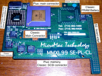
Now you're cooking! When I get a chance I'll put the digital calipers on the MicroMac board (assuming I find it anytime soon) to give you the offsets of the two connectors. It shouldn't be critical as connector installation is an either/or proposition.


ZaneKaminski

Well-known member
Can a PLCC device go in the socket upside-down? What does the socket on the bottom for the Classic look like?

There is a bit of a problem. I have to have a lot more circuitry on my board than on the MicroMac board, which has some severe space constraints. I can only expand it to the left.

SEClassicPlus.png

If I drop Classic compatibility, I can fill in the Classic PRAM battery, floppy connector, and main connector holes, widen the gap between the PDS-96 and DIP-64, and expand the board to the left. But it still may be difficult. 


Trash80toHP_Mini

NIGHT STALKER
Somebody just scored a Total Systems Gemini Accelerator for the Plus. That board is just about as big a footprint as an SE/Plus board can get. I'll see if I can find the thread and ask for some detailed pictures. I've never seen one other than in the ads and magazine reviews of Accelerators.

Go larger with your board and don't worry about the Classic, it's a turd that doesn't really warrant any polishing. :p


Trash80toHP_Mini

NIGHT STALKER
May wonders ever cease? I finally found Daystar's PowerCache adapter tree graphic!

ViBPwx.jpg.8b59828661706157c42fe274d3e4e19d.jpg


Diagram pre-dates the LCIII, the adapter for which is not shown.

This would be why you would design your 68030 board to interface with the IIci Cache Slot. Anyone with a PowerCache Card and wishing their further upgrade to their SE/30 or other supported Mac already has such an adapter.

Cloning the SE/30 and IIsi adapters would be a pet project of mine. If only I could get one into my grubby little paws!  }:)


Trash80toHP_Mini

NIGHT STALKER
Larger board = more $$$$.

More $$$ = less people purchasing. 
True, if a just a tad simplistic, there are serious trade offs to be considered:

What percentage of completed unit cost does the PCB actually represent?

Adding a bit of size for the dual connector implementation doubles +- the potential user base?

Don't know how the numbers might work out, but I'd hazard a guess that building two different designs for Plus and SE might be costlier in many ways.

techknight, was it you that once specified the function of the FPGA(?) implementation on the SE/30 and IIsi PowerCache adapters? Might that have been bbraun? In any case, I'd love to hear that explanation again. ;D


ZaneKaminski

Well-known member
Rather than the IIci slot, why not NuBus? A NuBus card might have a bit less bandwidth than a PDS card but would be compatible with a dozen models. The cards could programmed to speak either NuBus or 68030 bus, selectable by a jumper. The pin layout of the Euro-DIN 96 would be for NuBus, but there would exist an SE/30 and a IIci adapter that would rearrange the signals so the cars could speak 68030 bus.

Edit: wait no, the NuBus cards don't have enough pins to speak 68030. It could probably be done with just one or two ICs on the adapter card

 
Last edited by a moderator:

ZaneKaminski

Well-known member
I don't think I'm going to be able to do a card that works on both Plus and SE PDS, though. It just isn't cost-effective. There's not enough room for a bunch of level shifters and 3 TQFP-100 chips in between the paralleled PDS and 68000 DIP-64. I could do it in 6 layers, I think, but then that defeats the low-cost part. More layers also doesn't solve the problem of where to place the (numerous) connectors so they're accessible in the Plus and SE, and then the MIPI-DSI and USB 2.0 HS signals have pretty strict routing requirements, which are hard to achieve when space is constrained. So mechanically, I question whether the feature level I'm aiming for is possible for a card compatible with Plus and SE.

Trash, you've definitely convinced me to do a Plus board, though, so I will get on that. I'll try and make each as small as possible in order to reduce the cost.

 
Last edited by a moderator:

Trash80toHP_Mini

NIGHT STALKER
You don't necessarily need to design a Plus specific board if you take a page out of DayStar's book. Design a simple, "L" shaped (fat "T" shaped?) adapter PCB for the traces from 68000 socket thruholes to the PDS thruholes. You can use directly soldered header pin strips as a low profile board interconnect on the SE PDS side after installing the 68000 socket under the adapter and putting electrical tape over the protruding socket pins.

It's late, I hope that's clear enough.  |)  


Trash80toHP_Mini

NIGHT STALKER
Rather than the IIci slot, why not NuBus?
NuBus Accelerators like Radius' Rocket require on board memory to get around the multiplexed 10MHz signaling limitations. The PDS spec has full access to system memory at full bandwidth.

Having no provision for breakout from the case and less power budget than Apple's PDS spec/definition, the IIci Cache Slot remains as close as it gets to a standardized PDS. Very few of Apple's '030 (or any other) PDS implementations are the same, but all that I know of can be hoodwinked into thinking they're a IIci Cache Slot


ZaneKaminski

Well-known member
As long as a NuBus card can access video memory/VRAM, read the ROM, and access the peripherals (chipset and NuBus), I think it's doable. I dunno anything about NuBus though, other than that it's 32-bit, A/D multiplexed, and multi-master. The emulator is designed to use mostly its own RAM anyway, only writing-through for video accesses and waiting for I/O accesses to be completed over the 68000 bus.

The difficult problem to solve with an adapter is that the adapter must ensure that the peripheral connectors are accessible through the chassis. I'll see if it's possible.


ZaneKaminski

Well-known member
The Radius Rocket is the only NuBus based Accelerator that comes to mind. There were scads of PDS based Accelerators  .  .  .

.  .  .  do the math! ;)
Well this is new hardware development. Back in the day, logic cost more and they didn't have the luxury of accelerating the Macintosh with a custom-programmed 68000 emulator. There are some restrictions when you're running a real 680x0 that don't have to exist when you program a modern CPU or design your own core to do the task of executing 68000 instructions.

Months ago, for example, thetechknight was talking about the difficulties in performing synchronous peripheral accesses with a faster 68000. He said that most accelerators for the 68000 compacts emulate the peripherals that must be accessed synchronously according to the ECLK. That problem just doesn't exist when emulating the CPU. Certain timing restrictions like that can be eased.

So I think doing a NuBus accelerator is as doable as any other bus interface. The only tricky part will be dual-mode operation for the IIci and SE/30, where the card can pass through something easily convertible to the 68030 bus. But that's in the future.

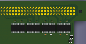
My progress tonight on the level-shifter area layout for Mac SE:

Screen Shot 2016-11-27 at 10.00.04 PM.png

I dunno what the rest of the board will look like, but I'm pretty sure the level shifters will need to be right next to the PDS lol.


ZaneKaminski

Well-known member
By the way, in case anyone is wondering, these address and data lines I've routed in the image aren't fast enough to need length-matching. The entire length of the PDS is like 10 cm, and the signals will propagate at 60 picoseconds per cm or so, so the entire length of the PDS is traversed in 600 picoseconds. For the Mac Plus and SE, at 7.83 MHz, a cycle takes ~128 nanoseconds, so 600 picoseconds like 1.7 degrees (out of 360) in the cycle. So uhh, that seems good. The level shifters impose a larger delay anyway.

IIci is the fastest Mac (in terms of bus speed) I plan could ever be supported. At 24 MHz, a cycle takes up 40 nanoseconds meaning that the same 600 picosecond figure is 5.4 degrees of a cycle. Hmm. Maybe boards for the IIci will have to put a tighter constraint on the skew between different lines and the signal propagation delay in general.

 
Top