I'm working on the schematic redraw, and I have an idea for connecting the ~OE pins on the DRAM ICs like the Mac Classic RAM expansion card without adding any new ICs. I'd like to hear opinions from others as the approach splits memory across the two DRAM ICs in a funny way.
The Mac Classic RAM expansion card Builder68 linked in a previous reply uses an AND gate on the two ~CAS lines (upper and lower bytes) for each DRAM, and the output of the AND gate is used to control the ~OE pins on each DRAM. To summarize the function: For each DRAM IC, if
either the upper or lower ~CAS line is asserted, the ~OE pin is asserted on the IC. Only the corresponding upper or lower byte will actually output data. Apparently, this allows for EDO style DRAM ICs to be used in place of FPM.

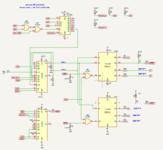
On my schematic, ~MCAS0F and ~MCAS1F could be connected to an AND gate to feed the ~OE pin for the DRAM IC which will receive those two ~CAS lines. The same could be done for ~MCAS2F and ~MCAS3F to the other DRAM IC. Scroll to the bottom of this reply to see it drawn on a schematic.

After some further thought, it occurred to me that in this design those four ~MCAS#F are derived from the 512K system's ~CAS0 and ~CAS1 lines. If the purpose of the AND gate is to combine two of the ~MCAS#F lines, why not skip it and drive the ~OE pins on the DRAM ICs with the 512K system's ~CAS0 and ~CAS1 for each of the two DRAM ICs directly? The downside to this is I wouldn't be able to take ~MCAS0F & ~MCAS1F to one DRAM IC and ~MCAS2F & MCAS3F to the other DRAM IC.
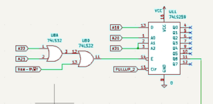
Take a look at the truth table for the 74LS138 which generates the ~MCAS#F signals. When ~CAS0 is asserted, either ~MCAS0F or ~MCAS2F will be asserted depending on the state of A21 or if the video hardware is accessing memory. Similarly, ~CAS1 drives either ~MCAS1F or ~MCAS3F. Thus, to drive the ~OE line for a DRAM IC from ~CAS0, that DRAM IC should be receiving ~MCAS0F and ~MCAS2F.

This means the DRAM IC containing the lower byte of the first 2MB of memory will also contain the lower byte for the second 2MB of memory. The other DRAM IC will contain the upper bytes for both the first and second 2MBs of memory. To summarize, instead of one 2MB 16-bit DRAM IC containing the first 2MB of memory (both upper and lower bytes) and another IC containing the second 2MB, one DRAM IC contains the lower bytes for all 4MB and the other IC contains the upper bytes for all 4MB. This doesn't seem so bad, except that it almost defeats the purpose for 16-bit DRAM ICs. Fortunately, the Mac 512K's RAM hardware only accesses one byte at a time, meaning either an upper or a lower byte, and never all 16-bits at once.
This is what it would look like:

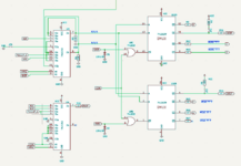
Compare that to how I would have expected or wanted the schematic to be:

It seems like a minor difference, and I think either way would work just fine. Does saving one IC (and more propagation delay) justify complicating the schematic? The method without the AND gate would certainly make troubleshooting a faulty DRAM IC difficult since either IC is responsible for the entire 4MB memory (upper or lower bytes, of course). Granted there are only two DRAM ICs, so it's a 50/50 shot at which one could be the hypothetical problem.