• Updated 2023-07-12: Hello, Guest! Welcome back, and be sure to check out this follow-up post about our outage a week or so ago.

Serious proposal: accelerator and peripheral expansion system

ZaneKaminski

Well-known member
The STM32H7 isn't up to dynamic translation of blocks of code (i.e. group of instructions following a jump target). It's just not powerful enough to translate while also interpreting at a good speed. Multiple cores are helpful for this.

The penalty for not translating is an indirect jump per instruction executed, which imo is kinda bad. But what we can do is translate some predefined blocks in the ROM into Thumb-2 at startup. That will allow the emulator to go through ROM routines really quickly, not having to jump and possibly flush the pipeline in between every instruction.


ZaneKaminski

Well-known member
Someone asked a few weeks ago about a schedule for the project. I think I can now say that The Macintosh SE and Plus accelerators will be completed in one and a half to two years. Hopefully, I am hoping that once I make more progress on the software in particular that other developers will be interested in collaborating on support for other machines. I'm done with my preliminary work now, in terms of figuring out how the system should be structured and operate. Soon I will post a new schematic along with new block diagram images for the hardware and put the source files on GitHub.

Today I started learning Verilog. Previously I had only used the sort of graphical block diagram tools in Altera Quartus II.

After the schematic is finished, the next deliverables will be the PCB design, a proof of concept version of the emulation engine, which will be one or more Thumb-2 assembly source files, and then block diagram and state machine pictures for the internal functional units in the bus glue FPGA.


techfury90

Well-known member
If you want my honest opinion, I would focus on taking an off-the-shelf Zynq board (I noticed Zynq was discussed before) and develop a NuBus/PDS "carrier card" to fit it on to. By doing this, you avoid all the difficulties involved with designing a Zynq board, for the most part. I should note that I'm currently chasing down this particular path once my board ever gets here. For now, it'll be a bit of a prototype playground for me to explore various possibilities for new expansion options.

 
Last edited by a moderator:

ZaneKaminski

Well-known member
If you want my honest opinion, I would focus on taking an off-the-shelf Zynq board (I noticed Zynq was discussed before) and develop a NuBus/PDS "carrier card" to fit it on to. By doing this, you avoid all the difficulties involved with designing a Zynq board, for the most part. I should note that I'm currently chasing down this particular path once my board ever gets here. For now, it'll be a bit of a prototype playground for me to explore various possibilities for new expansion options.
Too expensive though. Those modules are $150 at least, and then the PDS board will still be fairly costly. I'd do the Snapdragon module before anything designed to carry a large, clumsy module like the Zynq-7020, and I'm sure I could get better performance from a JIT translating emulator running on the Snapdragon 410.


ZaneKaminski

Well-known member
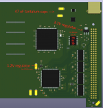
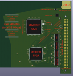
The project has been coming along nicely. I annotated an image that shows my current progress:

Screen Shot 2017-01-01 at 4.54.41 PM.png

One new "performance feature" is that I've switched to two using SDRAMs. The routing for this is substantially harder than for a "point-to-point" system with just one SDRAM, but I can manage it. The advantage is that there are not 32-bit 200 MHz SDR SDRAM chips available. So I have to use two 16-bit chips to achieve the requisite 200 MHz.

The board will have micro-USB, not the full-size USB-A as shown in the image. That saves quite a bit of space in an area which needs it.


ZaneKaminski

Well-known member
My friend (an adamant android fanboy), told me the same just now. I'll look into the prices. It's funny to mix technologies from different eras. Someone will one day find a Macintosh equipped with a "Maccelerator" and be totally confused.

However, I thought I could get by with just the OTG functionality of the micro-USB. The "peripheral board" could have a mini-USB. microB-to-miniB OTG cables are common. To get a USB receptacle, buy a $3 OTG connector thingy.


ZaneKaminski

Well-known member
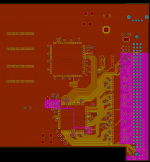
Some more work on the power stuff on the SE board from yesterday and today:

Screen Shot 2017-01-03 at 3.21.54 AM.png

This image shows my progress on the internal power layer. The pink represents areas in the the internal power plane. The stuff on the right is 5 volts, and the snakey area under the FPGA is for its 1.2 volt core supply:

Screen Shot 2017-01-04 at 1.37.58 AM.png

Nothing but tantalum caps on the board, so there will be no problems with leakage.

Talking about leakage, maybe PRAM chip emulation would be a good idea. The Maccelerator could store the PRAM contents in its onboard flash, so no need for the battery.


tt

Well-known member
Zane, I am not up to the particulars of this project, but it sounds really interesting and to answer your initial question, I'm interested in your future product. Is it more of an emulator than an accelerator board? 


ZaneKaminski

Well-known member
Zane, I am not up to the particulars of this project, but it sounds really interesting and to answer your initial question, I'm interested in your future product. Is it more of an emulator than an accelerator board? 
Well, the Maccelerator is an accelerator in the sense that the purpose is to go into a Macintosh and make it run faster. On the other hand, it has neither a hard 680x0 or an FPGA capable of hosting a 680x0 core. Instead, 68000 instructions are executed under emulation on a fast (400 MHz dual-issue ARMv7-M) microcontroller. So it's both.

The one thing that the Maccelerator is not designed to do is provide robust emulation of the rest of the Macintosh chipset. Emulators like Mini vMac have to have this component or else they would just be a 68000 emulator, not really a Mac emulator. Maybe some chipset functions can be emulated or bypassed to improve them (as I mentioned in my previous post about the PRAM), but definitely not everything.

Edit: by the way, the block diagrams and design given in the initial post are quite out-of-date compared to the current design. Very soon I will make a new thread and post the latest information in the first page.

 
Last edited by a moderator:

tt

Well-known member
Is there a major difference in supporting 100 vs 10 Mbps?

The one thing that the Maccelerator is not designed to do is provide robust emulation of the rest of the Macintosh chipset. Emulators like Mini vMac have to have this component or else they would just be a 68000 emulator, not really a Mac emulator. Maybe some chipset functions can be emulated or bypassed to improve them (as I mentioned in my previous post about the PRAM), but definitely not everything.
Would support for 68000 be similar to existing emulators like Basilisk vMac? Their emulation does have issues with fully supporting programs like the real hardware. The battery also helps keep time, but I guess you can use NTP to auto update every boot.


techfury90

Well-known member
100 is probably not worth it. I suspect that no 68k Mac can even saturate 10mbps. My A1200 with a 3Com 589 (Probably the best 10M PCMCIA card ever) can only do about 2 Mbps max with a 40MHz 030. I sincerely doubt that even an 840AV could saturate 10.

The limitation was definitely in the processor, because prism2.device with a WaveLAN got the exact same results.

 
Last edited by a moderator:

ZaneKaminski

Well-known member
Most 100 Mbit/sec Ethernet transceivers use the "Media-Independent Interface" (MII) or the "Reduced-pin-count Media-Independent Interface" (RMII) to talk to their host . Even the RMII interface has 10 signals to route. I'm running out of I/O pins on the STM32H7, so I was hoping to get a 10 Mbit/sec transceiver that supported an SPI interface, which would require only 4 signals. Turns out that there do exist such chips, but they are generally more expensive and larger than the 100 Mbit/sec chips supporting RMII. Oh well. I'll do 100 Mbit/sec. Maybe I will need to upgrade the STM32H7 to the larger 208-pin version, up from 176 pins.


cb88

Well-known member
That makes sense about the DDR QSPI....I saw DDR and immediately thought SDRAM.

The proprietary Apollo core does much better than 1 IPC ... IIRC it does more like 4 instructions per cycle max and averaging around 2.5. .... It throws alot of FPGA resources at the problem http://www.apollo-core.com/index.htm?page=features. You could probably do some of those optimizations on a 68k core... but not all (they dropped some less used features I think).

Tantalum caps can go bad as well... best to use ceramic where you can.

 
Last edited by a moderator:

Gorgonops

Moderator
Staff member
The one thing that the Maccelerator is not designed to do is provide robust emulation of the rest of the Macintosh chipset. Emulators like Mini vMac have to have this component or else they would just be a 68000 emulator, not really a Mac emulator. Maybe some chipset functions can be emulated or bypassed to improve them (as I mentioned in my previous post about the PRAM), but definitely not everything.
Actually, to some extent most Macintosh emulators targeted at the classic MacOS *do* bypass emulating some, if not most of the chipset functions. BasiliskII does this to a greater extent than vMac does, but both leverage a system by which they dynamically patch the Macintosh ROM to replace drivers for certain hardware with direct simplified calls to the emulation container. (For instance, both emulators use essentially the same ROM hack to replace the floppy driver with direct calls to the disk image handling system of the emulator; neither does *any* low-level emulation of the IWM chip for floppy-sized images and "mass storage", IE, hard-drive size images, are handled through the same driver, not via SCSI or IDE emulation. Basilisk goes further than vMac and leverages similar methods to replace the video, sound, and network drivers, which is why it's able to handle driving arbitrarily-sized 24-bit color desktop windows instead of being limited to the video capabilities of any one real Mac.) This is one of the things that makes me a little skeptical that you're going to much be able to exceed the performance of an emulator like Basilisk even if you're "just" doing the CPU; unlike, say, an Amiga emulator BasiliskII doesn't sit there spinning a lot of CPU time trying to emulate peripherals or the chipset in anything approaching a cycle-accurate way.


ZaneKaminski

Well-known member
Well the basic steps required to execute an instruction which has already been decoded are:

  1. Fetch the decoded instruction from the decoded instruction cache array.
  2. Take off the top 10 bits of the decode instruction and use that as an index to branch-and-link into the instruction implementation table stored in ITCM.
  3. The implementation of the instructions is executed against the MC68000 state structure, memory tree structure, etc. This includes incrementing the PC, accessing memory, doing register operations, etc.
  4. Control returns to the calling address stored in the link register.
  5. The calling function branches back to fetching the next instruction decode and the process starts again on the next instruction.
However, it's a little more complicated when the instruction has not already been decoded:

  1. Fetch the decoded instruction from the decoded instruction cache array.
  2. Since the instruction has not already been decoded, the cached value is 0x00000000. The top 10 bits are all 0, and this is used as an index into the implementation jump table.
  3. The first entry in the implementation jump table is the translation method, which decodes the instruction. This is slooooow. We don't want to do this more than we have to so the result is cached in the instruction decode cache table.
  4. The translation method returns control back to the calling function without changing the PC. Therefore the instruction is essentially retried.
  5. The calling function branches back to fetching the "next" instruction decode (actually retrying) and the process starts again.
  6. Fetch the decoded instruction from the decoded instruction cache array.
  7. Take off the top 10 bits of the decode instruction and use that as an index to branch-and-link into the instruction implementation table stored in ITCM.
  8. The implementation of the instructions is executed against the MC68000 state structure, memory tree structure, etc. This includes incrementing the PC, accessing memory, doing register operations, etc.
  9. Control returns to the calling address stored in the link register.
  10. The calling function branches back to fetching the next instruction decode and the process starts again on the next instruction.
Now for the implementations:

  • Register-register ops can be implemented without a jump and without ever stalling the pipeline.
  • Read accesses to memory may require a jump or otherwise induce a stall.
  • Write access to memory also may stall, but additionally, when writing to the main memory cache, the corresponding location in the instruction decode cache has to be invalidated, i.e. written to 0x00000000.
Now, I have totaled up all of the instructions and addressing modes, and there are nearly 800 that need to have separate implementations in ARMv7-M assembly. That's the hard (or maybe just time-consuming) part. Since there are so many, naturally we should expect little help from the branch predictor, etc. when jumping into the implementation routine. The Cortex-M7's pipeline is only 6 stages long though, I believe.

So the process of actually executing the instructions actually not that hard or slow as long as the code isn't terribly self-modifying. May I also note that the STM32H7 with 200 MHz 32-bit SDRAM has 400x more memory bandwidth than a Macintosh Plus. This "kernel" certainly can run 10x faster than an 8 MHz 68000 on an STM32H7 at 400 MHz. Of course, if you wrap this "kernel" that I have described up in an inefficiently-structured program, the process of emulation could be very slow. So the rest of the program has to be structured in a way that's favorable to the caches, branch predictor, banks and CAS latency of the SDRAM chips, etc.
 

ZaneKaminski

Well-known member
Would support for 68000 be similar to existing emulators like Basilisk vMac? Their emulation does have issues with fully supporting programs like the real hardware.
Honestly, I have not studied Basilisk II at all, and Mini vMac only briefly. So I don't know how their 68000 emulation works, but I imagine it's similar to the scheme I have come up with, other than the fact that my design is to be run "on top" of a working Macintosh and its chipset.

The entire RAM of the Macintosh will be stored in the Maccelerator and never actually written back to the Mac's memory (with the exception of video and peripheral accesses), so many instructions can be executed in the amount of time required by an actual 68000 for a single memory access. On that note, it's important to realize that my SDRAM setup has a peak throughput of 6.4 Gbit/sec, compared to 16 Mbit/sec for the Plus, and 24 Mbit/sec for the SE. So the 400x greater memory bandwidth is instrumental in achieving my goal of 10x faster than the Plus.

If you read my original post, there was discussion of a "translating emulator" or "JIT" or "dynamic recompilation" approach that I said could achieve 100x better performance than the 68000 compacts, but on a more powerful processor than I'm currently using. Right now, the architecture I am working on supports only 68000 models, and would basically give an insufficient boost to 68020+ systems, since they are quite a bit faster than the 68000 systems. In the future, I may develop the a faster and more expensive accelerator for 68020/68030 systems.

However, I think that a mode in which the instruction timing of the Macintosh Plus is emulated can be implemented, so users can use the Maccelerator's peripheral functionality without the acceleration.


ZaneKaminski

Well-known member
Register-register operations have a straightforward implementation, but then there are instructions that perform some reading or writing of memory, actually most do this since it's CISC. There are also branch instructions which require a more complex implementation.

Now when accessing memory, there is this concept of different "targets" of the access depending on the address. Some accesses are to be conducted over the 68000 bus. Others may involve reading from or writing to arrays in the memory of the STM32H7/SDRAM. In order to categorize these accesses, we need a tree structure.

In order to traverse the tree structure, we divide the 24-bit address into three 8-bit pieces, the high, middle, and low bytes. The high and middle bytes are used as indices into the doubly-indirect tree. What's found there is a structure containing four function pointers (total of 16 bytes). Each structure basically tells how to access the given 256-byte region of the 68000's address space. The function pointers go to routines for loading, storing, and executing code from the given region of memory. 

So to execute a load or store operation (possibly in the course of executing a more complicated, CISC-y instruction), compute the target address, then use that to go into the tree structure. Then branch-and-link to the routine implementing the load/store. That routine can look in an array, use the qSPI interface to talk on the bus, whatever.

To execute a branch instruction, compute the target address, use it to go into the tree structure, then branch to the routine for executing instructions in that area of memory. That's where the "basic steps required to execute an instruction" I gave in the post before last should be implemented.

Actually that procedure for executing an instruction only applies to instructions stored in main RAM, which is cached in the Maccelerator's SDRAM. A slightly different procedure should be implemented for executing code from something which is not cached (e.g. a peripheral card with a ROM).

 
Last edited by a moderator:

ZaneKaminski

Well-known member
Now there will be a lot of branching and stalling the pipeline and branch misprediction and all that, but let me point out:

The STM32H7, at peak, delivers 800 MIPS, compared to the Macintosh Plus, which delivers only 1 MIPS at most. Similarly, the STM32H7's SDRAM interface has a peak throughput of 6.4 Gbit/sec, compared to less than 16 Mbit/sec for the Macintosh Plus. So it's very possible to achieve performance 10x greater than these machines with this setup.

JIT-ing each jump target basically reduces the number of jumps performed in the course of emulation by two per instruction, so that's where the performance advantage of the JIT comes in, and you can also combine instructions, etc. for greater gains. The 68000 Maccelerators will not have JIT. It's necessary though for 68020+ to achieve the right performance.

Compared to the Apollo core, no, this method is probably 8-10x slower. But look at their prices: http://orders.apollo-accelerators.com. 250 or 300 EUR! I am aiming for 150 USD at the most for this one, and 220 USD at most for the 68020+ one with the Snapdragon and the JIT if I ever make it.

 
Last edited by a moderator:
Top