• Updated 2023-07-12: Hello, Guest! Welcome back, and be sure to check out this follow-up post about our outage a week or so ago.

Early Macintosh home brew 4MB memory upgrade board development

Builder68

Well-known member
I also tried the above configuration but with the RA9F generation in place to utilize the entire 2 MB of connected memory. This resulted in a decent looking screen during the power on tests, but it failed to complete them. The screen still has bad pixels here and there which indicate bad or missing bits. The power on tests take much more time which tracks since it’s 4x as much memory.


View attachment 74266

I thought I would look at the RAM-RD signal on the logic board’s memory output buffers compared to the RAM-R/~W signal and a ~CAS signal. Once my oscilloscope probes were connected, I found the power on BONG to be very distorted, and the screen was distorted as well. I narrowed it down to the RAM-R/~W signal which is used by the RAM ICs as a write enable, and my implementation uses it to control the data input buffers. Switching my probe from 1x to 10x helped drastically, but still had a negative effect on the system. It seems that this signal is very much affected by outside influence, even a high impedance one!

I wonder if the delay of my data input buffers being driven by this signal is right on the cusp of being outside acceptable timing tolerance, and perhaps the added capacitance of the long leads, breadboard, and oscilloscope probe is pushing it over the boundary.

I’m not sure what to do with that thought, since I’m pretty certain I need those buffers. Maybe there’s a way to generate a logically equivalent signal which occurs a little sooner? Or maybe the added capacitance is keeping it low longer than it should be, and I should gate it with another signal to ensure that it goes high sooner?

I just hope this particular rabbit hole is fruitful.
I remember Adam Black saying in one of his latest videos that the reason we see a clean black screen with the Sad Mac icon is because the ROM directly controls the display at that point. It bypasses the RAM and writes to the screen itself. When we see the Sad Mac icon over something else , it means at least the Mac is able to write something to the screen using RAM access. So, its better when you see those vertical lines than nothing
 
Last edited:

Builder68

Well-known member
To discard high impedances and interferences you would have to make a prototype using an universal PCB Soldering Circuit Board
 

Golden Potato

Well-known member
I should note that at one point I thought that perhaps the RAM-R/~W line was being overburdened, so I clipped the leg on R33 which goes to the logic board’s RAM ICs and tapped it at that point instead. This left only my two buffers and the two 1 MB DRAM ICs as the only loads. It made little to no difference.
 

Builder68

Well-known member
I also tried the above configuration but with the RA9F generation in place to utilize the entire 2 MB of connected memory. This resulted in a decent looking screen during the power on tests, but it failed to complete them. The screen still has bad pixels here and there which indicate bad or missing bits. The power on tests take much more time which tracks since it’s 4x as much memory.


View attachment 74266

I thought I would look at the RAM-RD signal on the logic board’s memory output buffers compared to the RAM-R/~W signal and a ~CAS signal. Once my oscilloscope probes were connected, I found the power on BONG to be very distorted, and the screen was distorted as well. I narrowed it down to the RAM-R/~W signal which is used by the RAM ICs as a write enable, and my implementation uses it to control the data input buffers. Switching my probe from 1x to 10x helped drastically, but still had a negative effect on the system. It seems that this signal is very much affected by outside influence, even a high impedance one!

I wonder if the delay of my data input buffers being driven by this signal is right on the cusp of being outside acceptable timing tolerance, and perhaps the added capacitance of the long leads, breadboard, and oscilloscope probe is pushing it over the boundary.

I’m not sure what to do with that thought, since I’m pretty certain I need those buffers. Maybe there’s a way to generate a logically equivalent signal which occurs a little sooner? Or maybe the added capacitance is keeping it low longer than it should be, and I should gate it with another signal to ensure that it goes high sooner?

I just hope this particular rabbit hole is fruitful.
Wow! I think you're almost there! It seems you're finally on the right track. Did you try smoothing or reinforcing the RAM-R/~W signal? It might be worth adding pull-up/down resistors to see if there's any change. At least, it would be interesting to see how it affects the number of bad pixels shown on the screen.

Also, I think you're probably right about those finicky tricks the MacSnap design implements. Perhaps their purpose is to make signal timing more accurate, or perhaps to make them less susceptible to external interference?

BTW, that Sad Mac error code I had it once, and it was due to poor connections at solder joints of J7. It has nothing to do with RAM, it means illegal instructions, address on the CPU. That's good news, some garbage due to poor signals and interference it may corrupting the CPU data bus

Anyway, I really believe the latest test shows your design works! There's little to nothing left to try at this point. Ultimately, you could try implementing as many of those tricks from the MacSnap design as possible, but I concede based on your explanations that it might not change the outcome at all. Perhaps it's time to make a prototype PCB of your design (I'd use a universal through-hole type, nothing fancy).
 
Last edited:

Golden Potato

Well-known member
Wow! I think you're almost there! It seems you're finally on the right track. Did you try smoothing or reinforcing the RAM-R/~W signal? It might be worth adding pull-up/down resistors to see if there's any change. At least, it would be interesting to see how it affects the number of bad pixels shown on the screen.

Also, I think you're probably right about those finicky tricks the MacSnap design implements. Perhaps their purpose is to make signal timing more accurate, or perhaps to make them less susceptible to external interference?

BTW, that Sad Mac error code I had it once, and it was due to poor connections at solder joints of J7. It has nothing to do with RAM, it means illegal instructions, address on the CPU. That's good news, some garbage due to poor signals and interference it may corrupting the CPU data bus

Anyway, I really believe the latest test shows your design works! There's little to nothing left to try at this point. Ultimately, you could try implementing as many of those tricks from the MacSnap design as possible, but I concede based on your explanations that it might not change the outcome at all. Perhaps it's time to make a prototype PCB of your design (I'd use a universal through-hole type, nothing fancy).
I wouldn't say my design works quite yet. I took nearly the entire design out of the circuit. Haha

I do think we should sprinkle in elements from the MacSnap design, but for now I'm still at the very beginning of trying to just get external 512K working.
 

Golden Potato

Well-known member
Damn. They're right, and it applies to the Mac 512K as well. The truth table I posted in this reply shows that during video access, the DRAM is given row address values from VA0-VA7 for ~RAS (C2M high). If the video circuit cycles through these addresses in a counter, and we can assume the logic board's DRAM is refreshed in RAS only mode, then the DRAM is given 256 cycles for refresh. That lines up with what those folks said in that post as well as the datasheet for the 256K chips in the Mac 512K.

The DRAM ICs I've been playing with require 1024 refresh cycles : 16 ms according to their datasheet. Same dilemma for the AS4C1M16F5 16-bit ICs you recommended in a previous post. I think this is going to be a major problem :/
 

Golden Potato

Well-known member
If refresh is a hang-up, why not just use SRAM? Here's an example I found that seems like it could work: https://www.digikey.com/en/products/detail/alliance-memory-inc/AS6C4008-55SINTR/4498663
If soldering SOPs is no fun, there are some SOJ and DIP options too, but at higher cost.
That could be an option. No refresh necessary but requires nearly 20 address lines. The speed is probably just fine though. They may even be fast enough to allow for some prop delays through latches if we wanted to continue using the RA0F-RA8F (or even RA9F) lines and use latches to save their state on the falling edge of ~RAS and ~CAS. That could save us from having to tap nearly 20 address lines off the CPU!
 

Golden Potato

Well-known member
That could be an option. No refresh necessary but requires nearly 20 address lines. The speed is probably just fine though. They may even be fast enough to allow for some prop delays through latches if we wanted to continue using the RA0F-RA8F (or even RA9F) lines and use latches to save their state on the falling edge of ~RAS and ~CAS. That could save us from having to tap nearly 20 address lines off the CPU!
Could probably get away with just two of these bad boys right herr. We could use just two 8 bit latches for RA0-RA7 and forget about RA8. The benefit would be that it could be compatible with 128K boards. Although It seems like people are more interested in restoring them back to 128K than upgrading them. A17 and A18 would then require being tapped directly on the logic board as A19, A20, and A21 already will.

The upper and lower bytes are individually controlled so one can read or write to the lower byte, upper byte, or both. Just as the system’s DRAM is implemented. It seems almost so easy that I must be overlooking something.

We would still need to use data input address latches, and I think I’ve had issues with that just trying to get 512K of DRAM working on the breadboard.
 

Builder68

Well-known member
Damn. They're right, and it applies to the Mac 512K as well. The truth table I posted in this reply shows that during video access, the DRAM is given row address values from VA0-VA7 for ~RAS (C2M high). If the video circuit cycles through these addresses in a counter, and we can assume the logic board's DRAM is refreshed in RAS only mode, then the DRAM is given 256 cycles for refresh. That lines up with what those folks said in that post as well as the datasheet for the 256K chips in the Mac 512K.

The DRAM ICs I've been playing with require 1024 refresh cycles : 16 ms according to their datasheet. Same dilemma for the AS4C1M16F5 16-bit ICs you recommended in a previous post. I think this is going to be a major problem :/
I think there is a problem, but not sure about the exact maximum number cycles is given to DRAM to refresh. Otherwise, the 1 MB SiMMS for the Mac Plus wouldn't work. Each SIMM have 8/9 ´44256 of 128KB (256Kb x 4 Bits), 512 refresh cycles / 8 ms. Those SIMM´s with an extra IC (9th) is for parity, which I believe read somewhere the early Macs ignores.
 
Last edited:

Builder68

Well-known member
Damn editing time haha... This completes the previous post


I think there's a problem, but I'm not sure about the exact maximum number of refresh cycles required for DRAM. Otherwise, the 1 MB SIMMs for the Mac Plus wouldn't work.

Each SIMM likely contains eight or nine IC´s DRAM chips that require 512 refresh cycles every 8 milliseconds.

The ninth chip (if present) is for parity checking, which I believe early Macs ignore.

In this old thread, someone suggests that some DRAM ICs with 1024 refresh cycles might be backward compatible with those requiring 512 cycles. Early Macs and Apple IIs frequently refer to this limitation as the number of rows that can be read and rewritten within a specific timeframe. The threshold for these machines seems to be 512 rows. So don't throw to the trash your dram IC´s yet!
 

Builder68

Well-known member
I found this and it seems worth giving a shot. Basically, it shows how to trigger extra refresh cycles.

What they are doing is adding a CAS before each RAS that isn't a memory access cycle, and therefore creating a bunch of "CAS before RAS" or (automatic) refresh cycles in which the chips do not need (disregard the state of) the address lines, and use their internal refresh address counters instead.

One caveat exists: Find on the Mac system an equivalent signal to their "REF signal", that changes more frequently than CAS signal.

I've checked the datasheets, and the DRAM ICs you're using do support "CAS before RAS." The IC I proposed also supports it.
 
Last edited:

Golden Potato

Well-known member
Damn editing time haha... This completes the previous post


I think there's a problem, but I'm not sure about the exact maximum number of refresh cycles required for DRAM. Otherwise, the 1 MB SIMMs for the Mac Plus wouldn't work.

Each SIMM likely contains eight or nine IC´s DRAM chips that require 512 refresh cycles every 8 milliseconds.

The ninth chip (if present) is for parity checking, which I believe early Macs ignore.

In this old thread, someone suggests that some DRAM ICs with 1024 refresh cycles might be backward compatible with those requiring 512 cycles. Early Macs and Apple IIs frequently refer to this limitation as the number of rows that can be read and rewritten within a specific timeframe. The threshold for these machines seems to be 512 rows. So don't throw to the trash your dram IC´s yet!
I’ll dig into the Mac Plus schematics a little deeper later, but at a glance it looks like the Mac Plus does provide 9 varying row addresses which would be sufficient for a DRAM with 512 rows to refresh. The Mac 512K and 128K only provide 8 varying row addresses which only refreshes 256 rows, which is compatible with the DRAM in the Mac 512K.

I’m unsure if the DMA implemented on the Mac Plus is used in memory refresh, video access to RAM, or something else?
 

Golden Potato

Well-known member
I found this and it seems worth giving a shot. Basically, it shows how to trigger extra refresh cycles.

What they are doing is adding a CAS before each RAS that isn't a memory access cycle, and therefore creating a bunch of "CAS before RAS" or (automatic) refresh cycles in which the chips do not need (disregard the state of) the address lines, and use their internal refresh address counters instead.

One caveat exists: Find on the Mac system an equivalent signal to their "REF signal", that changes more frequently than CAS signal.

I've checked the datasheets, and the DRAM ICs you're using do support "CAS before RAS." The IC I proposed also supports it.
This seems like a possible approach with enough research and experimentation. Have you looked into hidden refresh? It looks like it’s pretty much the same as CAS before RAS except the data output remains valid on the DRAM outputs in hidden refresh. Not sure if that would be required or not.
 

Builder68

Well-known member
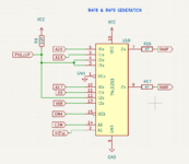
There seems to be an issue with the memory address bus. With more than 512KB of RAM, RAF8 is no longer the Least Significant Bit (LSB). Instead, RAF9 has become the LSB. Therefore, I guess RAF8 & RAF9 should be generated in the same way the Mac Plus does.

1718395976216.png
 

Builder68

Well-known member
The limitation is more significant. Even generating RAF8 and RAF9 signals like the Mac Plus does, there are other limitations. The Mac Plus introduces a more complex memory manager logic by newer combinatorial GAL equations (ICs BMU2, CAS).

Taking into account this limitation, with the MAC512K only DRAM ICs with a 9-bit memory address bus can be used.

The Mac 512K can only access chunks of 512KB at a time. Using the Macsnap design and six 256Kb x 16-bit DRAM ICs (plus the system DRAM), a 2MB homebrew expansion is still possible.

For a 4MB expansion board, fourteen 256Kb x 16-bit DRAM ICs and eight pairs of CAS signals would be needed.

Additionally, the Input Buffers from the Golden Potato design need to be implemented.
 
Last edited:

Builder68

Well-known member
The limitation is more significant. Even generating RAF8 and RAF9 signals like the Mac Plus does, there are other limitations. The Mac Plus introduces a more complex memory manager logic by newer combinatorial GAL equations (ICs BMU2, CAS).

Taking into account this limitation, with the MAC512K only DRAM ICs with a 9-bit memory address bus can be used.

The Mac 512K can only access chunks of 512KB at a time. Using the Macsnap design and six 256Kb x 16-bit DRAM ICs (plus the system DRAM), a 2MB homebrew expansion is still possible.

For a 4MB expansion board, fourteen 256Kb x 16-bit DRAM ICs and eight pairs of CAS signals would be needed.

Additionally, the Input Buffers from the Golden Potato design need to be implemented.
I made a mistake calculating the quantity of DRAM IC´s. For 1.5 Mbytes, 3 IC´s (2 Mbytes including system DRAM). For 3.5 Mbytes, 7 IC´s
 
Last edited:

Golden Potato

Well-known member
There seems to be an issue with the memory address bus. With more than 512KB of RAM, RAF8 is no longer the Least Significant Bit (LSB). Instead, RAF9 has become the LSB. Therefore, I guess RAF8 & RAF9 should be generated in the same way the Mac Plus does.

View attachment 74762
Did you mean to say most significant bit? The LSB would be RA0 corresponding to either A1 or A9 depending on C2M’s state. Or VA0 or VA8 if video is accessing memory.

I don’t understand what the problem is? For the original 128K Mac, there were only eight RAM address lines. RA7 was the MSB which corresponds to A8 or A16 depending on C2M’s state. Or VA7 or S5 if video is accessing memory. When they created the 512K upgrade, they implemented the additional ‘253 to multiplex A17 and A18 to create RA8. This caused no problems, and RA9 is proposed to be created the same way, so I’m not sure about the problem you describe?

I think one could completely scramble the RAM address lines before connecting them to the DRAM, and as long as it was consistent for all DRAM, it wouldn’t matter. They only care that every row is refreshed within the refresh cycle window, and the system only cares that bytes written to RAM remain where ever they are stored until read back from the same location.

I could be wrong, and if so please feel free to correct me!

The address signals I’m referring to come straight from the truth table in my previous reply here: https://68kmla.org/bb/index.php?thr...y-upgrade-board-development.47308/post-533221
 
Last edited:

Golden Potato

Well-known member
The limitation is more significant. Even generating RAF8 and RAF9 signals like the Mac Plus does, there are other limitations. The Mac Plus introduces a more complex memory manager logic by newer combinatorial GAL equations (ICs BMU2, CAS).

Taking into account this limitation, with the MAC512K only DRAM ICs with a 9-bit memory address bus can be used.

The Mac 512K can only access chunks of 512KB at a time. Using the Macsnap design and six 256Kb x 16-bit DRAM ICs (plus the system DRAM), a 2MB homebrew expansion is still possible.

For a 4MB expansion board, fourteen 256Kb x 16-bit DRAM ICs and eight pairs of CAS signals would be needed.

Additionally, the Input Buffers from the Golden Potato design need to be implemented.
Just for fun: If one were to stick with the original size DRAM ICs of which the Mac 512K consists, it would take a whopping 64 ICs! But the 16 ICs onboard could be kept in service, so only an additional 48 is needed. I think something from my notes in my first post was close to correct for creating the CAS lines. A required change would be to make it so that CAS0 derivatives could be asserted at the same time as CAS1 derivatives, rather than only one or the other at a time. It would then be 512K chunks as you said, not 256K chunks as I wrote.

Check out the bottom half of this pic from that post:
 
Top