You are using an out of date browser. It may not display this or other websites correctly.
You should upgrade or use an alternative browser.
You should upgrade or use an alternative browser.
Early Macintosh home brew 4MB memory upgrade board development
- Thread starter Golden Potato
- Start date
Yes, you're absolutely right MSB/LSB concept. I apologize for the confusion.Did you mean to say most significant bit? The LSB would be RA0 corresponding to either A1 or A9 depending on C2M’s state. Or VA0 or VA8 if video is accessing memory.
I don’t understand what the problem is? For the original 128K Mac, there were only eight RAM address lines. RA7 was the MSB which corresponds to A8 or A16 depending on C2M’s state. Or VA7 or S5 if video is accessing memory. When they created the 512K upgrade, they implemented the additional ‘253 to multiplex A17 and A18 to create RA8. This caused no problems, and RA9 is proposed to be created the same way, so I’m not sure about the problem you describe?
I think one could completely scramble the RAM address lines before connecting them to the DRAM, and as long as it was consistent for all DRAM, it wouldn’t matter. They only care that every row is refreshed within the refresh cycle window, and the system only cares that bytes written to RAM remain where ever they are stored until read back from the same location.
I could be wrong, and if so please feel free to correct me!
The address signals I’m referring to come straight from the truth table in my previous reply here: https://68kmla.org/bb/index.php?thr...y-upgrade-board-development.47308/post-533221
VA8 (Used as input with A9, A17 to generate RAF8 in the 74253) is the ninth bit of a 12-bit video address counter (VA0-VA11) generated by those 74393´s.
S5 is a pull-up resistor in the Mac Plus schematic.
The 12-bit video access counter is scrambled with the DRAM memory address bus. This "scrambling" logic in the 12-bit counter is identical across the Plus/128K/512K Macs (using 74LS393s and 74LS257s) except for RAF8 generation (the final stage of the 74LS253). Perhaps the video access counter plays also a role in generating refresh cycles. This is a reasonable guess, as video address counters in older PC systems were often used for DRAM refresh to avoid CPU overhead. The Mac Plus generates 512 refresh cycles, while the 128K/512K Macs only generate 256 cycles. See the potential connection with the way RAF8 is created?
Moving on from RAF8, 10-bit DRAM ICs won't work unless the combinatorial GAL equation stored in the "CAS" IC from the Mac Plus is fully understood. Even then, additional circuitry would be necessary to create CAS lines for 1MB RAM banks. This highlights another limitation: the 512K Mac only accesses RAM in 512KB chunks.
Assuming the logic was specifically designed for 256 refresh cycles, some additional circuitry would be needed to generate up to 512 cycles. I suspect this modification would be less complex than adapting for 10-bit DRAM ICs.
Therefore, my conclusion is that 256 cycles are generated for each 512KB memory bank for DRAM refresh. I believe the generation of these cycles is related to the 12-bit video address counter. For fun, I've ordered some 512-cycle 9-bit DRAM ICs to test this theory in practice.
Golden Potato
Well-known member
Indeed, the video circuitry is providing the refresh functionality on the early Macs. I understand what you are saying regarding the connection of these video address lines creating the limitation of only 256 cycles for refresh on the Mac 128/512K, and the benefit the Mac Plus has in its video address line connections to provide 512 cycles for refresh.The 12-bit video access counter is scrambled with the DRAM memory address bus. This "scrambling" logic in the 12-bit counter is identical across the Plus/128K/512K Macs (using 74LS393s and 74LS257s) except for RAF8 generation (the final stage of the 74LS253). Perhaps the video access counter plays also a role in generating refresh cycles. This is a reasonable guess, as video address counters in older PC systems were often used for DRAM refresh to avoid CPU overhead. The Mac Plus generates 512 refresh cycles, while the 128K/512K Macs only generate 256 cycles. See the potential connection with the way RAF8 is created?
I went ahead and redrew the truth tables for the RAM addresses for the Mac 512K along with one for the Mac Plus based on the schematics to easily see the differences you explained in an easy to see format.
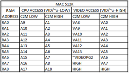
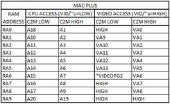
Then here they are again with the differences highlighted. You can pretty much ignore RA9 in this instance since that is entirely unique to the Mac Plus (for now!).
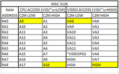
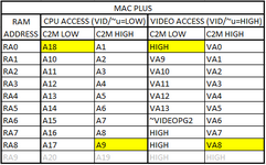
The relevant difference is that VA8 and HIGH from RA0 and RA8 are swapped, so when C2M is high, there are nine bits of VAx lines going to RA0-RA8 which creates 512 cycles for refresh. A9 and A18 had to follow suit for consistency, otherwise when the CPU writes to memory for video data, it would be all messed up.
If we wanted the Mac 512K to natively create 512 cycles for memory refresh, we could cut a trace or two (or socket the ICs and bend legs out) and solder a couple bodge wires to make it more like the Mac Plus in that regard. Not elegant by any means, but it should work!
Going beyond that, we could also hack it up further to create 1024 cycles of refresh which is required for the particular DRAM ICs I've got on the breadboard. Just move VA9 from RA1 to RA9 and replace where VA9 was at RA1 with a pull up resistor. A10 and A19 would need swapped at RA9 and RA1 to follow suit. This is what its truth table would look like:
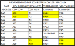
If this actually works, then for a cleaner mod: the IC responsible for RA0 & RA1 (U4F on the Mac 512K) and RA8 (U13G) could be removed, sockets installed, then the memory expansion board use pin headers to connect to the sockets. All of the signal swapping could be done on the expansion board, so no cutting logic board traces required! Also, the unused half of U13G could then be connected like the Mac Plus to create RA9, except with the additional changes above for 1024 refresh cycles.
Moving on from RAF8, 10-bit DRAM ICs won't work unless the combinatorial GAL equation stored in the "CAS" IC from the Mac Plus is fully understood. Even then, additional circuitry would be necessary to create CAS lines for 1MB RAM banks. This highlights another limitation: the 512K Mac only accesses RAM in 512KB chunks.
Assuming the logic was specifically designed for 256 refresh cycles, some additional circuitry would be needed to generate up to 512 cycles. I suspect this modification would be less complex than adapting for 10-bit DRAM ICs.
Therefore, my conclusion is that 256 cycles are generated for each 512KB memory bank for DRAM refresh. I believe the generation of these cycles is related to the 12-bit video address counter.
I think the modifications to change the refresh cycles should be straight forward as outlined above. As far as I know, the reason the 512K Mac accesses RAM in 512KB chunks is due to only being wired for 256 refresh cycles, which was a relic of the 128K Mac but still compatible with the DRAM ICs used in the 512K Mac. Changing to 512 or 1024 refresh cycles will allow the use of additional RAM address lines, which in turn means larger chunks of RAM access at one time. This thread has a few examples of multiplexing the logic board's CAS lines with upper system address lines to select more chunks, including the design you reverse engineered from the MacSnap board!
For fun, I've ordered some 512-cycle 9-bit DRAM ICs to test this theory in practice.
Let us all know how it works out! I appreciate the informational back-and-forth, as I've learned a TON. Especially considering I understood very little about DRAM access and refresh logic before venturing into this. I'm glad someone else is experimenting with the hardware too! Hopefully between the two of us, we can get this all sorted out soon and put together a working design schematic and PCB layout to share with the community!
Last edited:
Golden-Potato:
It sounds like you've made great progress in shedding light on understanding and proposing how to modify RAM address generation to 512 addresses on the 512k Macintosh!
Thank you very much for highlighting the differences between the Mac 512K and Mac Plus truth tables for RAM address generation. I completely overlooked the difference in RAF0 generation. Now, looking at the bigger picture, everything fits together and makes perfect sense!
By comparing the two truth tables side-by-side, we can also clearly see how hardware address decoding determines the screen memory location, and how it differs between the 128/512K Macs and the Mac Plus. Unlike the stock 512K Mac ROMs, the Mac Plus ROMs figure out how much memory is actually installed and then set ScreenBase (a pointer reference to a specific location below the top of memory for the screen buffer) appropriately.
I noticed the Mac Plus schematic shows RAF9 as NC (Not Connected) at the SIMM sockets. Must be an error since each SIMM needs ten address pins and eight data pins, otherwise 1MB SIMMs wouldn't work.
So, back to the point, by understanding the differences in how the Mac Plus generates 512 memory addresses for DRAM refresh compared to how the 128/512k Mac generates 256 addresses for DRAM refresh, we now know what to do to obtain 512 memory addresses for DRAM refresh for 10-bit memory address DRAM ICs with 512 refresh cycles: Generate RA0 and RA8 like the Mac Plus creates them, while keeping the same way to generate RA9 as is currently implemented in the prototype design.
However, would these modifications alone be enough to actually have 512 refresh cycles within a 1MB bank?
At this point, I'd like to share and go through my understanding so far on how the 512K/Plus Mac refreshes the DRAM ICs. Please feel free to add comments or corrections to clarify any misleading information or provide a clearer picture for everyone.
Early Macs (and Apple II machines too) use a method called "/RAS only refresh" for refreshing DRAM ICs.
Specifically, in 128/512K/Plus Macs, the TSM IC asserts the /RAS signal, which in conjunction with the appropriate RAM address (RA0-RA7/RA8) obtained from the circuitry that includes the LS393s, LS257s, and LS253s, performs a four-cycle (*) single read access to one of 256 (128/512K Macs) or 512 (Mac Plus) possible addresses of the row that needs refreshing on the address lines.
Unlike a normal read operation, the /CAS signal remains de-asserted (high) during /RAS-only refresh. The DRAM chip internally activates the specified row and performs the refresh operation, which involves re-reading the data from all the cells in the row and rewriting it back to maintain the charge.
After the refresh cycle is complete, the TSM IC deasserts /RAS, deactivating the row. (By the way, maybe it's time to buy one of those cheap portable oscilloscopes reviewed by BlackAdam on his YouTube channel... although my dream is to have a 4-channel RIGOL DHO 800 as my first oscilloscope!)
The 256/512 addresses accessed are arranged so that taken together they properly refresh all the memory. By accessing one of the 256/512 addresses around every 15 μs or less, all of the Mac's DRAM is refreshed in a time that should always be less than 4 ms for the system RAM on the 512k Mac (256 x 15 μs) or 8 ms (512 x 15 μs) for the 1MB SIMM RAM on the Mac Plus.
So, it's clear that we need two things to actually refresh a single row of 512: 1) /RAS asserted while /CAS lines remain unasserted, and 2) an appropriate RAM address generated to refresh the single row (remember that all cells belonging to that row will be automatically refreshed).
Since the TSM and BMU1 ICs are the same in all Early Macs (128/512/Plus), we can expect to have enough /RAS assertions for refreshing every fixed number of cycles, regardless of the implemented memory address manager circuitry. This means we should have the same quantity of /RAS assertions for refreshing in a continuous, predetermined time interval. Consequently, /RAS signal assertions should repeat at a fixed cycle rate consistently. Therefore, sometimes the CPU will be put on hold while waiting for the memory address bus to finish a refresh cycle (which is supposed to take 4 clock cycles to complete for a single row). On an IBM 8088 CPU, the read access signal occurs every 72 clock cycles. I haven't yet determined this timing for Early Macs.
As you said, the MacSnap Design provides us right away with the inputs and the exact circuitry to obtain CAS lines for 512KB banks (9-bit Address DRAM ICs).
On the other hand, now I understand that we don't necessarily need to reproduce the exact logic of the combinatorial equations stored in the CAS IC, since they are designed to allow selection between CAS lines for either 256KB banks or 1MB banks. However, we will definitely need to generate CAS lines for the size of the memory bank chosen for the RAM expansion board. Taking the /CAS signals generated by the MacSnap Design as an example, in theory we should be able to handle the system RAM with the first pair of /CAS lines (/CAS0F, /CAS1F). Then, if the RAM expansion is made of 1MB with 10-bit DRAM ICs with 512 refresh cycles, the /CAS line for the lower bytes would be: /CAS2F (AND) /CAS4F, and the /CAS line for the higher bytes would be: /CAS3F (AND) /CAS5F.
For now, I'd be very happy if I can make just one of the DRAM ICs I ordered work as a substitute for the system RAM. It should be easy to implement since the DRAM ICs are 262,144 words x 16 bits / 9-bit / 512 cycles. One of these ICs is equivalent to 16 system DRAM ICs, totaling 512KB. No need to create RAF9, but requires modifications to RAF0 and RAF8 to increment the addresses for refreshing to 512. It should work using the system CAS lines (by pulling the system DRAM's CAS inputs high). This is a good test for your input buffers as well. I promise to publish everything once I have it all ready for the test!
This whole process has been a fantastic learning experience for me too. Just like you, I barely understood DRAM and refresh logic before diving in. It's been incredible piecing together the puzzle with the information we have.
I'll definitely keep you updated on my progress with the single DRAM IC implementation. In the meantime, please share your results as well, no matter how small they may seem. Every piece of information helps us move closer to a solution.
I know there are some early Macintosh experts following our progress. I hope our determination to create a homebrew expansion for the Mac 128/512K using newer, high-density DRAM ICs motivates them to join in at some point!
Last edited:
Golden Potato
Well-known member
Builder68:
Rather than dedicated system down time for memory refresh, I assume that DRAM refresh on early Macs is accomplished by the video circuitry simply reading video data from RAM to draw to the CRT at ~60 Hz per entire screen draw. That's ~16 ms for the entire 14-bit video counter. Only the upper portion of memory holding the screen buffer is actually read, but the rest of the DRAM ICs should all get RAS only refresh as the RAS lines and RAM address lines are fed to all DRAM ICs.
Here's my math which should be double checked:
The above is an assumption of how the DRAM refresh is accomplished on early Macs, and I haven't proved it with measurements. I think it would be difficult to get a long enough oscilloscope capture to find evidence for this method of refresh or a dedicated refresh interval in the system. However, I suppose I could set up three channels on my scope: ~RAS, ~CAS0, & ~CAS1, and try to trigger when ~RAS is asserted and both CAS lines are unasserted. That could be tricky since that scenario is true for a short period at the start of every RAM read or write. I think I can set the trigger on my oscilloscope to delay for a certain amount of time. Hopefully, I can set it up to trigger at the point where one of the CAS lines should be asserted. If I can capture a lone ~RAS assertion with no CAS line activity, that would be strong evidence to support a dedicated RAS only refresh implementation outside of simple video memory reads.
Rather than dedicated system down time for memory refresh, I assume that DRAM refresh on early Macs is accomplished by the video circuitry simply reading video data from RAM to draw to the CRT at ~60 Hz per entire screen draw. That's ~16 ms for the entire 14-bit video counter. Only the upper portion of memory holding the screen buffer is actually read, but the rest of the DRAM ICs should all get RAS only refresh as the RAS lines and RAM address lines are fed to all DRAM ICs.
Here's my math which should be double checked:
- 14-bit video counter contains 16384 data locations accessed at a frequency of 60 Hz, so at least every 16 ms. (1 / 60 = ~0.016)
- Mac 512K DRAM ICs must be refreshed at least every 4 ms.
- In 4 ms, the video counter accesses 4096 data locations in memory (16384 / 16 x 4 = 4096).
- That means 16 complete refresh cycles (refresh cycle size of 256) occur every time the screen is redrawn. (4096 / 256 = 16)
The above is an assumption of how the DRAM refresh is accomplished on early Macs, and I haven't proved it with measurements. I think it would be difficult to get a long enough oscilloscope capture to find evidence for this method of refresh or a dedicated refresh interval in the system. However, I suppose I could set up three channels on my scope: ~RAS, ~CAS0, & ~CAS1, and try to trigger when ~RAS is asserted and both CAS lines are unasserted. That could be tricky since that scenario is true for a short period at the start of every RAM read or write. I think I can set the trigger on my oscilloscope to delay for a certain amount of time. Hopefully, I can set it up to trigger at the point where one of the CAS lines should be asserted. If I can capture a lone ~RAS assertion with no CAS line activity, that would be strong evidence to support a dedicated RAS only refresh implementation outside of simple video memory reads.
Golden Potato
Well-known member
Almost. According to this, the Mac uses 21888 bytes of memory for video RAM. That must be for both the main and alternate screen buffers selected by the VIDPG2 signal. So for one buffer written to the screen, it’s 21888 / 2 = 10944 locations accessed at a rate of 60 Hz. Crunching the numbers, I think the Mac 512K completes 10 refresh cycles (size 256) in one screen redraw.Here's my math which should be double checked:
- 14-bit video counter contains 16384 data locations accessed at a frequency of 60 Hz, so at least every 16 ms. (1 / 60 = ~0.016)
- Mac 512K DRAM ICs must be refreshed at least every 4 ms.
- In 4 ms, the video counter accesses 4096 data locations in memory (16384 / 16 x 4 = 4096).
- That means 16 complete refresh cycles (refresh cycle size of 256) occur every time the screen is redrawn. (4096 / 256 = 16)
Perhaps the video counter doesn’t count all the way to 16384 like I assumed?
You're right. DRAM refreshing task is not a dedicated system downtime for memory refresh. Perhaps my overly detailed explanation of the refresh mechanism "/RAS only" led you to believe otherwise.
Generally speaking, DRAM refresh operates more like a background task working in tandem with other two processes. Reading or writing data to RAM automatically refreshes the accessed rows, eliminating the need for dedicated refresh cycles in most cases.
Video refresh, which consumes a significant portion of CPU time (around a third in 128/512K Macs), provides another opportunity. The video address counter, used to track screen updates, is used to generate memory addresses for DRAM refresh, thereby piggybacking on the existing video access cycles and eliminating additional overhead.
This collaborative approach minimizes the impact of refresh on CPU performance. The downtime caused solely by DRAM refresh typically falls around 5% of total CPU time, and it further varies depending on the specific application's memory access patterns.
Programmers in the 1980s were well aware of this behavior and factored it into their coding practices.
I leaved here some interesting numbers I found that shows how the 128/512K Macs timing is built around the video timing.
The Mac timing is a bit odd and built around the Video timing.
- Base clock is 7.83 MHz (*2)
- Line frequency is 22.255 kHz.
- Thus a video line is exactly 352 clock cycles
- A 68k needs 4 cycles per read/write
- This gives 88 memory access slots
- One line is 512 pixel or 32 (16 bit) words
- CPU and video access RAM alternating during the first 64 access slots
- CPU gets 24 exclusive slots during horizontal retrace.
- CPU gets as well all slots during vertical retrace
- There are ~32,560 access slots in frame (Refresh is 60.14 Hz)
- There are 342 lines per screen
- Resulting in 342 x 32 = 10,944 video reads
- This leaves about 2/3rd for the CPU
- If the CPU would utilize memory at all times, the effective speed would be close to 5.2 MHz
- Since the 68k isn't, and it's only stopped when there is a memory access, effective speed is more like 6 MHz
Golden Potato
Well-known member
Oh okay, I must have misinterpreted you.You're right. DRAM refreshing task is not a dedicated system downtime for memory refresh. Perhaps my overly detailed explanation of the refresh mechanism "/RAS only" led you to believe otherwise.
Generally speaking, DRAM refresh operates more like a background task working in tandem with other two processes. Reading or writing data to RAM automatically refreshes the accessed rows, eliminating the need for dedicated refresh cycles in most cases.
Video refresh, which consumes a significant portion of CPU time (around a third in 128/512K Macs), provides another opportunity. The video address counter, used to track screen updates, is used to generate memory addresses for DRAM refresh, thereby piggybacking on the existing video access cycles and eliminating additional overhead.
This collaborative approach minimizes the impact of refresh on CPU performance. The downtime caused solely by DRAM refresh typically falls around 5% of total CPU time, and it further varies depending on the specific application's memory access patterns.
Programmers in the 1980s were well aware of this behavior and factored it into their coding practices.
I leaved here some interesting numbers I found that shows how the 128/512K Macs timing is built around the video timing.
The Mac timing is a bit odd and built around the Video timing.
- Base clock is 7.83 MHz (*2)
- Line frequency is 22.255 kHz.
- Thus a video line is exactly 352 clock cycles
- A 68k needs 4 cycles per read/write
- This gives 88 memory access slots
- One line is 512 pixel or 32 (16 bit) words
- CPU and video access RAM alternating during the first 64 access slots
- CPU gets 24 exclusive slots during horizontal retrace.
- CPU gets as well all slots during vertical retrace
- There are ~32,560 access slots in frame (Refresh is 60.14 Hz)
- There are 342 lines per screen
- Resulting in 342 x 32 = 10,944 video reads
- This leaves about 2/3rd for the CPU
- If the CPU would utilize memory at all times, the effective speed would be close to 5.2 MHz
- Since the 68k isn't, and it's only stopped when there is a memory access, effective speed is more like 6 MHz
Very interesting info!
Looking forward to the arrival of your DRAM and your experimentation. In reality, I won’t really have the time to play with my setup for a few weeks, but I might get the urge one night and lose a little sleep to try out the modified RAM address stuff.
I’m really glad you had the intuition to dig into why/how the Mac Plus RAM addressing differs from the Mac 128/512K. I had kind of accepted that they were different without truly understanding the differences and was just about ready to move to an SRAM based design.
Still waiting for the arrival of the new DRAM ICs.The relevant difference is that VA8 and HIGH from RA0 and RA8 are swapped, so when C2M is high, there are nine bits of VAx lines going to RA0-RA8 which creates 512 cycles for refresh. A9 and A18 had to follow suit for consistency, otherwise when the CPU writes to memory for video data, it would be all messed up.
In the meantime, I've been re-checking the Mac Plus and 512K schematics for any differences in the memory address interleaved logic. I found one more difference related to RA0 address generation:
- In the 512K Mac (U2F/LS257), A0 (pin #2) input is VA13.
- In the Mac Plus, the A0 input is a pull-up resistor (S5).
I've attached the schematics I'm using for reference. Perhaps someone with knowledge of these specific schematics could identify any errors they might contain.
Attachments
Last edited:
Golden Potato
Well-known member
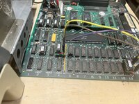
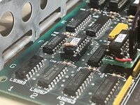
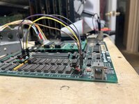
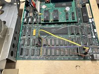
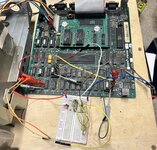
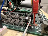
I played around with swapping those signals on U4F and U13G at first by cutting traces and wiring bodge wires, but decided to put together a couple little carrier boards which connect all the pins of the ICs back to the logic board except those which we want to try to swap. The pins to swap are connected to jumper pins to make it easy to go between stock and swapped.
As you can see, the system still works as expected with the pins swapped, but the audio is horribly destroyed. Theoretically, the video VA# lines going to the RAM circuit should now count sequentially from 0 to 511 instead of just counting sequentially from 0 to 256. Obviously, the VA# lines access addresses beyond these values, but sequentially accessed is key for /RAS-only refresh.
I’d like to get to the bottom of the sound circuit not agreeing with the signals being swapped before moving much further with the RAM IC stuff. Any ideas?
As an aside, I think I’d like to connect my USB logic analyzer to the RA# lines with enough other signals as permissives for triggering to see if I can capture a shot of the memory refresh due to video access in the case of stock connections and signals swapped as outlined above. That way, we can see proof of the system going from producing 256 cycles for refresh to 512.
View attachment IMG_5761.mov
As you can see, the system still works as expected with the pins swapped, but the audio is horribly destroyed. Theoretically, the video VA# lines going to the RAM circuit should now count sequentially from 0 to 511 instead of just counting sequentially from 0 to 256. Obviously, the VA# lines access addresses beyond these values, but sequentially accessed is key for /RAS-only refresh.
I’d like to get to the bottom of the sound circuit not agreeing with the signals being swapped before moving much further with the RAM IC stuff. Any ideas?
As an aside, I think I’d like to connect my USB logic analyzer to the RA# lines with enough other signals as permissives for triggering to see if I can capture a shot of the memory refresh due to video access in the case of stock connections and signals swapped as outlined above. That way, we can see proof of the system going from producing 256 cycles for refresh to 512.


View attachment IMG_5761.mov
I was about to write to you! I like very much the approach you've taken now of testing those modifications on RA0 and RA8 (CPU access / 74253´s) use solely the system memory. The results are very interesting.I played around with swapping those signals on U4F and U13G at first by cutting traces and wiring bodge wires, but decided to put together a couple little carrier boards which connect all the pins of the ICs back to the logic board except those which we want to try to swap. The pins to swap are connected to jumper pins to make it easy to go between stock and swapped.
Have you tried changing the signal on pin #2 of U2F from VA13 to S5 (Pull-Up)? I haven't thought thoroughly about these modifications yet, but it's worth trying since it definitely modifies RAM address bit RA0 for sound (on the 74257s), as it does in the Mac Plus.As you can see, the system still works as expected with the pins swapped, but the audio is horribly destroyed. Theoretically, the video VA# lines going to the RAM circuit should now count sequentially from 0 to 511 instead of just counting sequentially from 0 to 256. Obviously, the VA# lines access addresses beyond these values, but sequentially accessed is key for /RAS-only refresh.
I received those 16-bit/512KB/512 refresh cycle RAM ICs and finally was able to test them a couple of days ago with modifications to the RAM address bits RAS0 and RAS8 for CPU access to RAM (using 74253s). Instead of cutting traces, I decided to use an additional 74253 on the test board to generate RAS0 and RAS8 separately. I used CAS0 and CAS1 from the system, pulling the CAS signal tracks high to the system memory.
Well, the results are similar to, and a little better than, when you tried testing just your expansion RAM IC (RAS9 pulled high) and the input buffers with the system CAS signals.
I always had clean booting screens without any vertical lines, with a few bad pixels when the boot process succeeded. The startup completed successfully most of the time, displaying the floppy icon with a blinking question mark.
The main improvement was that 90% of the time the boot sequence completed successfully, the Mac remained running without crashing for as long as I observed it (waiting for a system disk, no SAD Mac Icon appears). I didn't try to boot any OS, as I was sure it would crash at some point.
On other occasions (to be honest, 50% of the boot attempts), the memory check stage didn't complete and produced the typical 3FXXXX error codes. I'm sure I had poor connections somewhere, so I can't be really sure if we have (or don't have) a timing problem with the input buffers at this point.
The boot chime always sounded distorted.
I took a more "dirty" approach to test the RAM expansion design. I soldered several sockets directly onto the ICs to make most of the connections to a test board using pin headers. (I don't recommend it!)
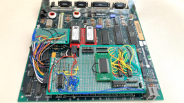
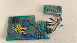
Just yesterday, I disassembled the connections to make several modifications to see if I could find what is causing those bad pixels. Here are some of the mods I want to attempt at some point (one at a time):
For the sound distortion, I will swap the VA13 signal on pin #2 of U2F IC to S5 to see if there is any improvement in the boot chime sound.
Open R33 leg to the system RAM ICs to discard the possibility that noise on the RAM-R~{W} signal is generated by the system RAM ICs. (If you try or have tried this, let me know the result)
CAS0 / CAS1 signals "ANDit" with the C2M as the MacSnap Board does. This will introduce some delay in the RAS to CAS time. Let's see if there's any improvement.
Generate an inverse signal of RAM-R-{W} with a 7404, and AND it with ~(RAMRD) to introduce some delay to the enabling of the added input buffers (74144s) with respect to the write enable of the expansion RAM.
Any feedback is welcome!
Golden Potato
Well-known member
I have not, and I recall you mentioning this difference previously, and I never really thought too much about it. I hadn't realized it was part of the sound circuit, and I just now noticed that it produces RA# lines which didn't make sense at first until I noticed it's only active during DMA access while the '253s are inactive. I don't quite fully understand how the memory access circuit for sound and speed control for the floppy drive works (which they share?), but in my head it seems that the CPU would put sound data into RAM via the '253s, then the sound hardware would read that data out via the '257s. Since swapping those signals affected RA0, it makes sense that a bit of data placed into RAM destined for the sound hardware accessed via RA0 with C2M low will be out of place. Instead of VA8, placing S5 (pull up) on pin 2 of U2F as you mentioned makes sense, but wouldn't VA8 need to go somewhere else, not just stay out of the picture? I'm looking at the schematic, and I'm just not seeing it anywhere else.Have you tried changing the signal on pin #2 of U2F from VA13 to S5 (Pull-Up)? I haven't thought thoroughly about these modifications yet, but it's worth trying since it definitely modifies RAM address bit RA0 for sound (on the 74257s), as it does in the Mac Plus.
So like you said, I think we should try removing VA8 from pin 2 on U2F and pulling the pin high. I don't fully understand it, but I can see how it might help.
In response to the rest of your message:
Great prototype build! I'm interested to see the results of the other mods you described. I recall when I did much with the RAM-RD/~WR signal things were very screwy. I think I did clip one lead from a resistor to remove it from the onboard DRAM, but I think it somehow made it worse??
Golden Potato
Well-known member
I test the prototype using the system's RA0 and RA8. Here are the results:
After restarting the Mac at least twice, the startup chime sounded as expected. (The first two times the chime sounds distorted, and boot process ends with the Sad Mac icon)
Most of the time, I could boot the OS from ROM (ROM-INATOR) or using Floppy Emu. I was even able to boot “Dark Castle” a couple of times before it crashed. Randomly appearing bad pixels and crashes time to time.
I'm cautiously optimistic, suspecting the stability issues might be due to insufficient power to drive the prototype board, poor connections, lack of proper grounding, parasitic capacitances, or interference.
Consistently, after disconnecting and reconnecting the logic board and AC power cord, I needed to restart the Mac several times to reach the happy Mac icon with a clear chime sound. It's as if something needs to be pre-charged with some residual voltage.
I suspect the way I deliver the 5VDC and ground is part of the problem. Maybe the bodge wires are insufficient for powering this RAM chip? Each of these RAM chips (AS4C256K16FO) consumes around 700 mA, while the 41256s consume about 30-40 mA each. That means a single one of these RAM chips consumes as much as sixteen 41256s!
Next test will be to gate CAS0 and CAS1 with C2M and see what changes...
Golden Potato
Well-known member
You could try adding some capacitors between +5V and GND near ICs on your prototype. Another thing could be any 74LS253s used on the prototype could be swapped with 74F253s dive that is what Apple used in the Mac. I believe the 74F series has a shorter propagation delay. That may not be the issue, but I suppose it’s worth trying?I test the prototype using the system's RA0 and RA8. Here are the results:
After restarting the Mac at least twice, the startup chime sounded as expected. (The first two times the chime sounds distorted, and boot process ends with the Sad Mac icon)
Most of the time, I could boot the OS from ROM (ROM-INATOR) or using Floppy Emu. I was even able to boot “Dark Castle” a couple of times before it crashed. Randomly appearing bad pixels and crashes time to time.
I'm cautiously optimistic, suspecting the stability issues might be due to insufficient power to drive the prototype board, poor connections, lack of proper grounding, parasitic capacitances, or interference.
Consistently, after disconnecting and reconnecting the logic board and AC power cord, I needed to restart the Mac several times to reach the happy Mac icon with a clear chime sound. It's as if something needs to be pre-charged with some residual voltage.
I suspect the way I deliver the 5VDC and ground is part of the problem. Maybe the bodge wires are insufficient for powering this RAM chip? Each of these RAM chips (AS4C256K16FO) consumes around 700 mA, while the 41256s consume about 30-40 mA each. That means a single one of these RAM chips consumes as much as sixteen 41256s!
Next test will be to gate CAS0 and CAS1 with C2M and see what changes...
I only used LS253s on my breadboard, but now that I desoldered and socketed U13G, I could move it to a breadboard and utilize the unused half to generate RA9.
It certainly seems like we’re getting close to cracking it!
I just added a 10uF capacitor for general decoupling. Also added a pair of 0.1 uF capacitors next to the 74LS244s. The distorted chime seems to be gone!. It looks like almost all boot attempts now reach the waiting floppy disk icon in one shot. However, I don't see any noticeable improvement with the bad pixels. Most, if not all, of the bad pixels appear when the CPU is doing some heavy task like reading data or launching an app.You could try adding some capacitors between +5V and GND near ICs on your prototype. Another thing could be any 74LS253s used on the prototype could be swapped with 74F253s dive that is what Apple used in the Mac. I believe the 74F series has a shorter propagation delay. That may not be the issue, but I suppose it’s worth trying?
I only used LS253s on my breadboard, but now that I desoldered and socketed U13G, I could move it to a breadboard and utilize the unused half to generate RA9.
It certainly seems like we’re getting close to cracking it!
We're making strides for sure, let's keep pushing.It certainly seems like we’re getting close to cracking it!
Remember that the prototype is currently using system RA0 and RA8. Therefore, the 74253 is not needed at this stage.Another thing could be any 74LS253s used on the prototype could be swapped with 74F253s dive that is what Apple used in the Mac. I believe the 74F series has a shorter propagation delay. That may not be the issue, but I suppose it’s worth trying?
Golden Potato
Well-known member
I finally figured out and fixed the sound issue with the 512 cycle refresh mod! As suspected, VA8 and HIGH being swapped between RA0 and RA8 results in some sound data being stored (initiated by the CPU) into a new location in memory, while the sound hardware for accessing memory is still expecting data at the old location. To visualize exactly how the sound hardware accesses memory, I added to the tables I previously made.
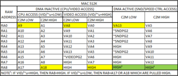
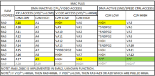
The differences are highlighted. Yellow highlight represents a known difference, and green represents an unknown. The Mac Plus table has gray text for RA9 to indicate that it isn't something the Mac 512K can be compared against.
The tables were expanded to include an additional logic input: DMA. The OE pins on the '253s are wired so they are only active when DMA is not occurring, which is anytime sound or floppy drive speed control is not accessing memory. One caveat is the '253 U13G which has its OE pin tied low, so it is always active. More on that later! The '257s OE pins are connected to active when DMA is occurring. They are the other source which creates the RA# lines, except they don't create anything for RA8 which is fully controlled by U13G.
On the Mac Plus, RA8 is created by a '253 and also as an output from BMU2. I don't know exactly what the logic in BMU2 does for RA8, but I took a guess which happened to work out.
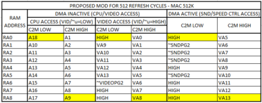
For RA0, lifting pin 2 on U2F and tying it high, which follows the thought that swapping VA8 for HIGH when DMA is inactive means that we must also swap VA13 for HIGH when DMA is active, is correct. I suspected the missing part was that we must reintroduce VA13 for RA8 when DMA is active, specifically when C2M is high.
I achieved this by implementing another multiplexor. I used a '253 because it's what I have, but it could have been a '257 like the rest of the sound hardware memory access circuit. I only used half of the IC, so one OE pin was tied high to disable it. The half that I used I connected similar to the Mac's '257s for the sound hardware as follows:
Pin 1 (OEa): ~DMA - only active when sound hardware is accessing memory
Pin 2 (S1): tied LOW - never select A3 or A2
Pin 3 (A3): tied LOW - not used
Pin 4 (A2): tied LOW - not used
Pin 5 (A1): VA13 - selected when C2M is high
Pin 6 (A0): tied HIGH - selected when C2M is low
Pin 6 (ZA): RA8
Other input pins except power: tied low
Other output pin: floating
The remaining issue is that U13G is always in control of RA8, and we must make room for the new multiplexor to take control when sound hardware needs to access memory. I did that the same way the rest of the system's '253s do: by taking the OE pin for the implemented half o the IC (pin 1) and connecting it to the DMA signal.
Here's the resulting table for this logic, highlights indicate a change from the stock Mac 512K:
View attachment IMG_5796.mov


The differences are highlighted. Yellow highlight represents a known difference, and green represents an unknown. The Mac Plus table has gray text for RA9 to indicate that it isn't something the Mac 512K can be compared against.
The tables were expanded to include an additional logic input: DMA. The OE pins on the '253s are wired so they are only active when DMA is not occurring, which is anytime sound or floppy drive speed control is not accessing memory. One caveat is the '253 U13G which has its OE pin tied low, so it is always active. More on that later! The '257s OE pins are connected to active when DMA is occurring. They are the other source which creates the RA# lines, except they don't create anything for RA8 which is fully controlled by U13G.
On the Mac Plus, RA8 is created by a '253 and also as an output from BMU2. I don't know exactly what the logic in BMU2 does for RA8, but I took a guess which happened to work out.
For RA0, lifting pin 2 on U2F and tying it high, which follows the thought that swapping VA8 for HIGH when DMA is inactive means that we must also swap VA13 for HIGH when DMA is active, is correct. I suspected the missing part was that we must reintroduce VA13 for RA8 when DMA is active, specifically when C2M is high.
I achieved this by implementing another multiplexor. I used a '253 because it's what I have, but it could have been a '257 like the rest of the sound hardware memory access circuit. I only used half of the IC, so one OE pin was tied high to disable it. The half that I used I connected similar to the Mac's '257s for the sound hardware as follows:
Pin 1 (OEa): ~DMA - only active when sound hardware is accessing memory
Pin 2 (S1): tied LOW - never select A3 or A2
Pin 3 (A3): tied LOW - not used
Pin 4 (A2): tied LOW - not used
Pin 5 (A1): VA13 - selected when C2M is high
Pin 6 (A0): tied HIGH - selected when C2M is low
Pin 6 (ZA): RA8
Other input pins except power: tied low
Other output pin: floating
The remaining issue is that U13G is always in control of RA8, and we must make room for the new multiplexor to take control when sound hardware needs to access memory. I did that the same way the rest of the system's '253s do: by taking the OE pin for the implemented half o the IC (pin 1) and connecting it to the DMA signal.
Here's the resulting table for this logic, highlights indicate a change from the stock Mac 512K:


View attachment IMG_5796.mov
Similar threads
- Replies
- 61
- Views
- 14K
- Replies
- 0
- Views
- 1K
- Replies
- 203
- Views
- 34K

