I have both great and not-so-great news...
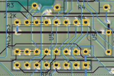
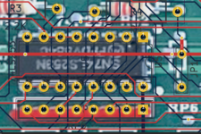
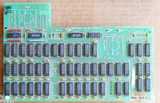
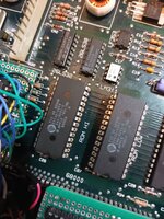
Finally, as you can see in the attached pictures, my Mac 512K is reporting 1 MB of RAM! Here's how I achieved this:
The prototype build utilizes SYSTEM RA0 and RA8. CAS lines are generated using a reverse-engineered MacSnap subcircuit, without the 150-ohm resistors (I opened System CAS at RP3). As with the MacSnap board 524, expansion RAM is the first bank (~MCAS0F, ~MCAS1F), and System RAM is the second (~MCAS2F, ~MCAS3F). I also implemented the 74259 and added a jumper selector to choose between ground and pin 11 as input to pin 15 of the 74253. Selecting ground allows the system to boot and report 1 MB, while selecting pin 11 also boots the system but only recognizes the first bank regardless of whether system RAM or expansion RAM is swapped.
It took extensive testing to identify a significant issue. The Mac hangs during OS startup (at the "Welcome to Macintosh" screen) when my ROM-INATOR board is installed (pin 15 of 74253 to ground). Using pin 11 of the 74259 allows booting but prevents recognition of the second memory bank.
The ROM-INATOR board uses A17, A18, and A19 as inputs. I suspect the conflict arises from A19.
View attachment 76624
View attachment 76625
View attachment 76626
There are some important takeaways to mention:
This RAM IC probably would be a great candidate to replace all system RAM at once on 128/512K Macs. To be 100% sure, it needs to be mounted on a future PCB and thoroughly tested beforehand.
The fact that the MacSnap design is not compatible with the ROM-INATOR is a setback.
The added output buffers seem to work flawlessly, and there appear to be no timing conflicts with the system RAM...


")