• Updated 2023-07-12: Hello, Guest! Welcome back, and be sure to check out this follow-up post about our outage a week or so ago.

Early Macintosh home brew 4MB memory upgrade board development

Golden Potato

Well-known member
This does not seem related to a problem with refresh cycles. The Mac always hangs at the same point, regardless of the OS version. It appears that the CPU is writing to a 'reserved' RAM space used by a ROM mirror, perhaps. The ROM-INATOR uses the entire address space, so an address conflict is more likely.
As far as I know, the ROMinator would only be selected when the system is accessing data in the ROM area of the address map, and RAM would not be selected. Same goes for vice-versa. The ICs are just not enabled unless their select logic allows them so. I'm not sure I understand what the issue could be.

The ROMinator requiring A17-A19 makes sense, since that was the unused (mirrored) portion of the address space in which the ROM is selected. The ROM also uses A1-A18, which overlaps with the address lines used by RAM as well, but that doesn't matter since RAM isn't selected unless the correct area of the memory map is being addressed.

I will admit I'm not familiar with the ROMinator, so I may be overlooking something.
 

Golden Potato

Well-known member
We have a proven CAS generation sub circuit design that certainly works (taken from the MacSnap Board), but it can only handle four banks of 512KB, and also we probably have a RAM IC that seems to be compatible with the Mac 512K's memory refreshing mechanism.

Of course, the ultimate goal is to reach 4MB. This first PCB with the simplest possible design will be a great accomplishment along the way.
Absolutely! :D
 

Golden Potato

Well-known member
Maybe I'm wrong, but using 4 CAS lines wouldn't mean the 512K Mac would read in banks of 1 MB instead of 512KB?. You would need to devise some circuitry to replicate certain tasks performed by the CAS IC on the Mac Plus to generate RAS/CAS signal cycles (and probably others) for banks of 1 MB.
Correct! That's why I mentioned RA9 generation: RA0-RA9 equates to 1MB on a DRAM IC, so only 4 banks and associated CAS lines required. It certainly seems to complicate things, and it tends to diverge from core elements of the MacSnap design in favor of leaning on elements of the Mac Plus design.

That's what I've had on my draft schematics all along, but I only have 4-bit DRAM ICs, so there are eight on the schematic. The goal would be 16-bit ICs, and only two of them!
 

Golden Potato

Well-known member
... and also we probably have a RAM IC that seems to be compatible with the Mac 512K's memory refreshing mechanism.

I'm still wary about this. In an unmodified Mac 512K, the only signal which isn't held high for RA8 while C2M is high (which is the state when RAS goes low, latching row addresses into DRAM) is the CPU accessing RAM via A18. There's no way the video or sound hardware can do it, so half of the rows of your DRAM will not be refreshed unless the program running on the CPU has a hand in it.

Maybe the system purposefully refreshes memory by CPU accesses to RAM, but the evidence presented by changes in design from the 512K -> Plus indicate video reads are providing this function. I'm thinking that this 512 cycle RAM getting refreshed without the video circuit doing so can be chalked up to good luck. This is why I suspect the ROMinator doesn't play nicely with it. Perhaps it's not doing the thing that just-so-happened to make it all work?
 
Last edited:

Builder68

Well-known member
I'm still wary about this. In an unmodified Mac 512K, the only signal which isn't held high for RA8 while C2M is high (which is the state when RAS goes low, latching row addresses into DRAM) is the CPU accessing RAM via A18. There's no way the video or sound hardware can do it, so half of the rows of your DRAM will not be refreshed unless the program running on the CPU has a hand in it.

Maybe the system purposefully refreshes memory by CPU accesses to RAM, but the evidence presented by changes in design from the 512K -> Plus indicate video reads are providing this function. I'm thinking that this 512 cycle RAM getting refreshed without the video circuit doing so can be chalked up to good luck. This is why I suspect the ROMinator doesn't play nicely with it. Perhaps it's not doing the thing that just-so-happened to make it all work?
I have a different theory about how the refresh mechanism works:

The refresh mechanism the 512K generates 256 addresses (RA0-RA7) to the lower 16-bit address word (CAS0, Row G of 8 41256´s ICs) first. That takes less than 4 ms.

Then, RA8 goes high and generates another 256 addresses (RA0-RA7), which are latched to the higher 16-bit address word (CAS1, Row F of 8 74256´s).

So every 41256 (1 bit) is refreshed at least every 4 ms, but from the new RAM IC (16 bits) perspective, it 'sees' 512 addresses generated sequentially (RA0-RA8) in less than 8 ms!

That could not be a coincidence, probably the designers of the 512K had in mind at some point to use DRAM IC´s of 512 refresh cycles, so they came up with a mechanism that would work for both types of RAM IC.
 
Last edited:

Builder68

Well-known member
I have a different theory about how the refresh mechanism works:

The refresh mechanism the 512K generates 256 addresses (RA0-RA7) to the lower 16-bit address word (CAS0, Row G of 8 41256´s ICs) first. That takes less than 4 ms.

Then, RA8 goes high and generates another 256 addresses (RA0-RA7), which are latched to the higher 16-bit address word (CAS1, Row F of 8 74256´s).

So every 41256 (1 bit) is refreshed at least every 4 ms, but from the new RAM IC (16 bits) perspective, it 'sees' 512 addresses generated sequentially (RA0-RA8) in less than 8 ms!

That could not be a coincidence, probably the designers of the 512K had in mind at some point to use DRAM IC´s of 512 refresh cycles, so they came up with a mechanism that would work for both types of RAM IC.
I made some errors in my previous post, please discard it!

Here is what I want really to say:

I have a different theory about how the refresh mechanism works:

The refresh mechanism in the 512K generates 256 addresses (RA0-RA7) to refresh the lower and higher 16-bit data (Row G and F of 8 41256´s ICs) at the same time. This takes less than 4 ms. Everything is clear up to this point right?

But from a RAM IC of 9-bit address with 512 refresh cycles (RA0-R8) perspective, things are seen like this:

Somehow RA8 must be toggling at least every 4 ms in perfect sync with the restart of the refresh counter (RA0-RA7).

So the new RAM IC (16 bits data, 9 address bits) "sees" 512 addresses generated sequentially (first the lower or higher 16-bit data for 4 ms, then the other lower or higher 16-bit data RA0-RA8 for another 4 ms) in less than 8 ms!

The way the refresh is done could not be a coincidence. Probably the designers of the 512K had in mind at some point to use DRAM ICs with 512 refresh cycles, so they came up with a mechanism that would work for both types of RAM IC.

Toggling of RA8 solely due to CPU or video access wouldn't be enough to accomplish a complete refresh of its 512 rows. It is simply not feasible. For sure, many rows would not be refreshed within an 8 ms period, and data corruption would occur instantly

I have let the Mac run with the OS for up to 30 minutes, and no hanging or crashing occurred.
 
Last edited:

Builder68

Well-known member
If you have the time and motivation, it would be nice to test swapping around those signals for the RA0 and RA8 generation to create 512 cycle refresh and test that with your ROMinator. I wouldn’t worry about swapping things to fix distorted audio for that test.
I will do that, that test could be very interesting!

Another interesting test would be to try my prototype build with the 512K stock ROM!. What type of ROM do you have installed on your 512K?
 
Last edited:

Golden Potato

Well-known member
I made some errors in my previous post, please discard it!

Here is what I want really to say:

I have a different theory about how the refresh mechanism works:

The refresh mechanism in the 512K generates 256 addresses (RA0-RA7) to refresh the lower and higher 16-bit data (Row G and F of 8 41256´s ICs) at the same time. This takes less than 4 ms. Everything is clear up to this point right?

But from a RAM IC of 9-bit address with 512 refresh cycles (RA0-R8) perspective, things are seen like this:

Somehow RA8 must be toggling at least every 4 ms in perfect sync with the restart of the refresh counter (RA0-RA7).

So the new RAM IC (16 bits data, 9 address bits) "sees" 512 addresses generated sequentially (first the lower or higher 16-bit data for 4 ms, then the other lower or higher 16-bit data RA0-RA8 for another 4 ms) in less than 8 ms!

The way the refresh is done could not be a coincidence. Probably the designers of the 512K had in mind at some point to use DRAM ICs with 512 refresh cycles, so they came up with a mechanism that would work for both types of RAM IC.

Toggling of RA8 solely due to CPU or video access wouldn't be enough to accomplish a complete refresh of its 512 rows. It is simply not feasible. For sure, many rows would not be refreshed within an 8 ms period, and data corruption would occur instantly

I have let the Mac run with the OS for up to 30 minutes, and no hanging or crashing occurred.
This is my understanding for refresh as well. The video circuit is counting sequentially for 256 rows via RA0-RA7. The video circuit can not toggle RA8, and it can only be accomplished by the CPU. The order doesn’t really matter so much as long as each row is refreshed every 4 ms. The CPU must have A18 low and access the lower 256 rows within 4 ms then it must have A18 high and access the upper 256 rows within 4 ms. A18 might toggle high and low sporadically throughout accessing the rows, but so long as all combinations of RA0-RA8 are accessed with 8ms, you DRAM would be happy. It must be driven by programming on the CPU, I just don’t know how to prove it.

Last night I tried probing A18 and triggering when C2M is high and RAS is low, which is when the DRAM would latch in a row address. Of course it triggers but sporadically, so I can’t tell exactly what the maximum amount of time passes between trigger events. This alone probably wouldn’t be enough evidence to say for sure how it’s working.

If the designers expected someone to use 512 refresh DRAM in the future, wouldn’t they have left the design as-is for the Mac Plus rather than modify the video circuitry (and audio circuitry to match) to create 512 consecutive row accesses (which is what its DRAM requires)?

I wish I knew what and how to probe various signals to prove or disprove this thought.
 

Golden Potato

Well-known member
I will do that, that test could be very interesting!

Another interesting test would be to try my prototype build with the 512K stock ROM!. What type of ROM do you have installed on your 512K?
My system has Mac Plus ROMs since it came with a contemporary SCSI upgrade board.

I would be interested in having a copy of your prototype to probe and test! If you get around to laying out a PCB, I would definitely order one and associated parts.

For the path (more like rabbit hole) I’m going down, I have some parts and protoboards on the way to solder up a prototype for DRAM with 10 address lines which will hopefully perform better than my old solder less breadboards.
 

Golden Potato

Well-known member
I could burn some stock ROMs, but the EEPROMs I have on hand are either too small or too large. I could use the larger ones and make adapter sockets though!
 

Builder68

Well-known member
This is my understanding for refresh as well. The video circuit is counting sequentially for 256 rows via RA0-RA7. The video circuit can not toggle RA8, and it can only be accomplished by the CPU. The order doesn’t really matter so much as long as each row is refreshed every 4 ms. The CPU must have A18 low and access the lower 256 rows within 4 ms then it must have A18 high and access the upper 256 rows within 4 ms. A18 might toggle high and low sporadically throughout accessing the rows, but so long as all combinations of RA0-RA8 are accessed with 8ms, you DRAM would be happy. It must be driven by programming on the CPU, I just don’t know how to prove it.

Last night I tried probing A18 and triggering when C2M is high and RAS is low, which is when the DRAM would latch in a row address. Of course it triggers but sporadically, so I can’t tell exactly what the maximum amount of time passes between trigger events. This alone probably wouldn’t be enough evidence to say for sure how it’s working.

If the designers expected someone to use 512 refresh DRAM in the future, wouldn’t they have left the design as-is for the Mac Plus rather than modify the video circuitry (and audio circuitry to match) to create 512 consecutive row accesses (which is what its DRAM requires)?

I wish I knew what and how to probe various signals to prove or disprove this thought.

After reseating the Mac Plus's stock ROM ICs a couple of times, I'm glad to report that I haven't had any crashes since!

I've been using the Mac for increasingly longer periods, and it's as stable as a rock. I can even run all versions of 'Speedometer' without any issues.

I'm very happy to finally be able to see the 'Flying Toasters' screen saver on my Mac 512Ke!
 

Builder68

Well-known member
A18 might toggle high and low sporadically throughout accessing the rows, but so long as all combinations of RA0-RA8 are accessed with 8ms, you DRAM would be happy. It must be driven by programming on the CPU, I just don’t know how to prove it.


If the designers expected someone to use 512 refresh DRAM in the future, wouldn’t they have left the design as-is for the Mac Plus rather than modify the video circuitry (and audio circuitry to match) to create 512 consecutive row accesses (which is what its DRAM requires)?

I wish I knew what and how to probe various signals to prove or disprove this thought.
Well, I think you've said something that makes a lot of sense. The 512Ke was intended to be a cheaper option than the Mac Plus. All performance tests show the Mac Plus is slightly faster than all previous models when it comes to CPU tasking.

What if the designers thought a cheaper and not so efficient way to introduce RAM ICs of 512 cycles was to implement some programming in the ROM that would consume some CPU time to adjust the refreshing to 512 cycles by manipulating A18? What if such routines existed in the ROM back in the 128/512K? (It would be very interesting to see if my prototype build could actually work with the 128/512K stock ROM.)

Perhaps the numbers never added up, so they opted to make the cheapest possible next version of the 512K and leave the 512Ke with exactly the same logic board (and same memory type) as the 128/512K, but the programming for memory refreshing remained in the newer ROM (only active when a 512K/E is detected).

With the Mac Plus, they redesigned the entire memory controller part, and in doing so, some of the routines (when the ROM detects a Mac Plus) were purged, possibly releasing some CPU time dedicated to memory refreshing. They also improved the buffering (74LS245) and created new signals to handle memory banks selectively of 256KB or 1 MB.

It's been a few hours now since the Mac has been running the "flying toasters" screen saver... still no crashes! I will leave it now with just the OS running in standby for a couple of hours and see what happens.
 
Last edited:

Builder68

Well-known member
It's been more than 12 hours since I put the prototype expansion memory to heavy use on my Mac 512k, and I'm happy to report that it's been rock solid! I've put it through the paces with everything from copying and formatting floppies to running the most demanding games, but it hasn't crashed or hung once. I'm really impressed with the stability so far, given the fact that the prototype build looks like a bunch of twisted cables and messy solder joints everywhere, haha!
 

Golden Potato

Well-known member
Well, I think you've said something that makes a lot of sense. The 512Ke was intended to be a cheaper option than the Mac Plus. All performance tests show the Mac Plus is slightly faster than all previous models when it comes to CPU tasking.

What if the designers thought a cheaper and not so efficient way to introduce RAM ICs of 512 cycles was to implement some programming in the ROM that would consume some CPU time to adjust the refreshing to 512 cycles by manipulating A18? What if such routines existed in the ROM back in the 128/512K? (It would be very interesting to see if my prototype build could actually work with the 128/512K stock ROM.)

Perhaps the numbers never added up, so they opted to make the cheapest possible next version of the 512K and leave the 512Ke with exactly the same logic board (and same memory type) as the 128/512K, but the programming for memory refreshing remained in the newer ROM (only active when a 512K/E is detected).

With the Mac Plus, they redesigned the entire memory controller part, and in doing so, some of the routines (when the ROM detects a Mac Plus) were purged, possibly releasing some CPU time dedicated to memory refreshing. They also improved the buffering (74LS245) and created new signals to handle memory banks selectively of 256KB or 1 MB.

It's been a few hours now since the Mac has been running the "flying toasters" screen saver... still no crashes! I will leave it now with just the OS running in standby for a couple of hours and see what happens.
Interesting postulation! I wonder if there’s a decent emulator with breakpoints and the ability to view memory addresses and disassembly for the early Macs? It would be awesome to dive in deep to see if we can identify something like that happening.
 

Golden Potato

Well-known member
It's been more than 12 hours since I put the prototype expansion memory to heavy use on my Mac 512k, and I'm happy to report that it's been rock solid! I've put it through the paces with everything from copying and formatting floppies to running the most demanding games, but it hasn't crashed or hung once. I'm really impressed with the stability so far, given the fact that the prototype build looks like a bunch of twisted cables and messy solder joints everywhere, haha!
This is so great! It seems super stable.

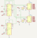
So I know it’s wayyyy too many ICs, but hear me out. You could take that MacSnap design and add another ‘253 (only half of it need be implemented) and hook it up just like the existing one but with A21 as its input. Then replace the ‘139 with two ‘138s. Instead of 2-to-4 demuxes, it becomes 3-to-8 demuxes. You could have a whopping 16 CAS lines for a full 4MB of RAM!
 

Golden Potato

Well-known member
This is so great! It seems super stable.

So I know it’s wayyyy too many ICs, but hear me out. You could take that MacSnap design and add another ‘253 (only half of it need be implemented) and hook it up just like the existing one but with A21 as its input. Then replace the ‘139 with two ‘138s. Instead of 2-to-4 demuxes, it becomes 3-to-8 demuxes. You could have a whopping 16 CAS lines for a full 4MB of RAM!
Something like this:
1723042196728.png
 

Golden Potato

Well-known member
Imagine using 128 256x1-bit DRAM ICs to build out 4MB! 😆

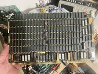
It would look something like this 4MB multibus card I have, except this card does parity checking, so it has 144 DRAM ICs. IMG_5866.jpeg
 

Builder68

Well-known member
I ran simulations of both CAS generation designs, one using 74139s and the other using 74138s, for eight memory banks.Both designs worked as expected for all possible combinations of A19 and A20, but both exhibited erratic behavior when A21 transitioned from floating to high and then to low, resulting in incorrect CAS line selection after the C2M, ~RAS, and VID/~u signal cycle sequence.

As expected, simply adding a hardware pull-up to A21 resolved the issue. A19 and A20 already have hardware pull-ups on the logic board. I hope adding this pull-up won't cause any other problems.

I've already carefully reassembled my Mac with the prototype installed. Is there any chance you could test pulling A21 high on your logic board to verify the Mac's operation?. Many thanks!

Anyway, just to be safe, I could add a 4N35 optocoupler to the PCB layout to isolate the A21 input to the CAS generation sub-circuit.
 
Last edited:
Top