Since the prototype build has worked so well (not even one crash or hang in all these days), I'm currently in the process of developing multiple PCB design proposals for the prototype build (3.5MB Memory expansion plus 512KB onboard memory, using system RA0 & RA8 only to simplify the circuitry as much as possible). To optimize costs, I'm requesting quotes from several PCB manufacturers to determine the most economical option. Any advice on this matter would be greatly appreciated. I'm using only modern components (SMD 0805 for capacitors and resistors, and SOIC 1.27 mm package for 74XX ICs).
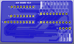
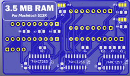
One of the proposals I like best is splitting the board into two parts. Due to the challenging placement of the connection points to the 74LS244 buffers, a single board design would result in significant wasted space. By separating the layout into a small board over the TSM IC and another board for the 74LS244s and the rightmost 41256 ICs, I believe it can achieve a more efficient and cost-effective design. I believe the only wires that would travel from one board to the other would be the CAS lines. I'd like to hear other perspectives on this as well.
A clear advantage of splitting the memory expansion is that the small TSM/BMU board would be dedicated to CAS signal generation. Any improvements would only require a new version of this board. The board with the 7 512KB RAM ICs and input buffers wouldn't need further revisions.
Last edited:


")
