Early Macintosh home brew 4MB memory upgrade board development

Golden Potato

Well-known member
Great news!.

BTW, I'm taking a closer look at those 150 ohm resistors. The MacSnap likely adds to the mainboard memory, so its function might be a kind of trick to override the original signals. Maybe I'm talking gibberish, but as far as I understand, a low value resistor in this configuration is more likely used to prioritize / reinforce the 74LS139's output by weakening any opposing signals rather than acting as a traditional pull-up resistor... Meaning if that 74LS139 goes high (unasserted), an opposite low CAS (asserted) signal coming from the mainboard circuitry will have a difficult time to be "seen". Perhaps both signals will always be in sync, and the purpose of the resistor is to provide enough current for the corresponding lower / upper 8 ICs on the mainboard... It puzzled me why use those resistors only with the CAS signals that go to the mainboard...
I think you’re exactly right. In the scenario you described when the logic board CAS is low, but the ‘139 output is high, a voltage divider is formed. To simplify, let’s say the system’s CAS output is perfectly 0 V, and let’s also say the high output of the ‘139 does not contribute to the circuit at this time (although it’s not, think of it as an open collector output just to really simplify things).

You have:
5 V -> 150 ohm -> 47 ohm -> DRAM IC CAS inputs -> logic board CAS resistor (47 ohm) -> 0 V (logic board CAS output low).

47 / (47+47+150) x 5 V = 0.96 V which, if the signal started out low, should theoretically not trigger the DRAM CAS inputs.

It still works for the case when the expansion board tries to drive the logic board’s DRAM CASF signals low since the respective CAS signal on the logic board will also be low as that’s the signal from which the expansion board’s CAS signal is derived. I don’t think it’s possible for the logic board’s CAS signal to be high when the respective CAS signal on the expansion board is low. I hope that wasn’t as confusing as I’m afraid I phrased it!
 

Builder68

Well-known member
I think you’re exactly right. In the scenario you described when the logic board CAS is low, but the ‘139 output is high, a voltage divider is formed. To simplify, let’s say the system’s CAS output is perfectly 0 V, and let’s also say the high output of the ‘139 does not contribute to the circuit at this time (although it’s not, think of it as an open collector output just to really simplify things).

You have:
5 V -> 150 ohm -> 47 ohm -> DRAM IC CAS inputs -> logic board CAS resistor (47 ohm) -> 0 V (logic board CAS output low).

47 / (47+47+150) x 5 V = 0.96 V which, if the signal started out low, should theoretically not trigger the DRAM CAS inputs.

It still works for the case when the expansion board tries to drive the logic board’s DRAM CASF signals low since the respective CAS signal on the logic board will also be low as that’s the signal from which the expansion board’s CAS signal is derived. I don’t think it’s possible for the logic board’s CAS signal to be high when the respective CAS signal on the expansion board is low. I hope that wasn’t as confusing as I’m afraid I phrased it!
Crystal clear, thank you very much for doing the calculations (I admit, I'm a bit lazy!). It's a finely tuned voltage divider to bring voltages within the limits of logical "1s" and "0s" in TTL technology. And yes, it should work even if the signals are out of sync.

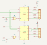
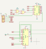
I'm attaching a new version of the CAS generation sub-circuit. I suspected something was amiss with the previous output at pin 7, since it had no connected trace. To identify the error, I had to trace all the CAS lines of the 48 6256 ICs. An RAF9 would need to be generated if, as intended, the 48 6256 DRAM ICs are replaced with newer, higher-density DRAM ICs. This RAF would specifically address the modification of the second 74LS253, where the A17 and A18 inputs from the original MacSnap configuration would be changed to A19 and A20.

Alright, Golden Potato's up! Let's see what magic they've cooked up in their updated design!
1716597254333.png1716595648136.png
 
Last edited:

Builder68

Well-known member
I guess that's it for MacSnap for now. Let's shift our focus to Golden Potato's ongoing homebrew design. It aims to reach 4Mb with just two DRAM ICs. We'll see how it integrates all this new input.
 

Golden Potato

Well-known member
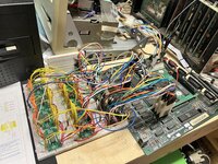
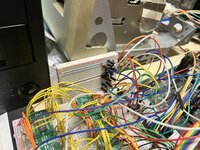
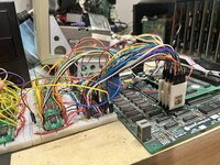
Since I hadn’t taken apart the original breadboard circuit, I’d only disconnected it from the logic board, last night I hooked it back up. I did add AND gates to the CAS output lines as I drew on a schematic in a previous reply. This was to allow the pair CAS0F and CAS1F or the pair CAS2F and CAS3F to be asserted at the same time if the logic board’s CAS0 and CAS1 signals are concurrently asserted.

As you can see, it still didn’t work. I wasn’t really expecting this bird’s nest to work for a variety of reasons including potential wiring mistakes, poor connections, and signal noise. Sure enough, the display noise changes when I hover my hand nearby. But there was definitely a change on the display compared to the previous attempt which would only allow the system to access the lower or upper byte of RAM but never both at once which definitely doesn’t work. So I’ll take that as progress!

I think there’s enough understanding regarding the early Mac’s memory circuit and tricks from the MacSnap to start drawing up a new schematic and laying out a proper prototype PCB. I’ll share the schematic after it’s done before laying out the PCB.

For now, enjoy some pics and clips of last night’s nonsense!


IMG_5130.jpeg

IMG_5131.jpeg


View attachment IMG_5141.mov


View attachment IMG_5142.mov
 

Builder68

Well-known member
Seeing how your hand affects the Mac display suggests interference and noise are likely minimal concerns. The breadboard should be capable of handling the Mac's frequency rates. Memory allocation or buffering problems seem more probable. It's possible there's an oversight in your design or faulty connections, but you're absolutely right to abandon testing on the current design.

To simplify troubleshooting, I recommend breaking the problem down into smaller steps. The key is to minimize connections initially and leverage a proven design like the Macsnap's memory management and buffering subcircuits.

The simplest approach would be to create a new schematic that completely replicates the Macsnap memory management and buffering subcircuits. This is a proven design with a high chance of success, even on a breadboard. I can definitely help you with any details about MacSnap traces in the images I provide before.

Unfortunately, generating the MacSnap truth tables is beyond my capabilities. Deciphering the 74LS259 behavior and the purpose of those pull-down resistors connected to the 74LS253 that bridges those inputs with the outputs was like deciphering ancient Greek!

To further minimize connections, start with just two of your DRAM ICs instead of eight. If successful, the Mac should recognize 1MB of RAM (512Kb from the system and 512Kb from your added DRAM). This will establish a solid foundation for comparison. You can then systematically introduce and test changes to your initial design. This could involve testing your RAM address handling and input buffering circuits, disabling the onboard RAM to see if it causes issues, and finally adjusting the DEMUX to generate only the CAS lines needed for expansion to 4MB using newer 1Mb x 16-bit ICs.
 
Last edited:

Builder68

Well-known member
Seeing how your hand affects the Mac display suggests interference and noise are likely minimal concerns. The breadboard should be capable of handling the Mac's frequency rates. Memory allocation or buffering problems seem more probable. It's possible there's an oversight in your design or faulty connections, but you're absolutely right to abandon testing on the current design.

To simplify troubleshooting, I recommend breaking the problem down into smaller steps. The key is to minimize connections initially and leverage a proven design like the Macsnap's memory management and buffering subcircuits.

The simplest approach would be to create a new schematic that completely replicates the Macsnap memory management and buffering subcircuits. This is a proven design with a high chance of success, even on a breadboard. I can definitely help you with any details about MacSnap traces in the images I provide before.

Unfortunately, generating the MacSnap truth tables is beyond my capabilities. Deciphering the 74LS259 behavior and the purpose of those pull-down resistors connected to the 74LS253 that bridges those inputs with the outputs was like deciphering ancient Greek!

To further minimize connections, start with just two of your DRAM ICs instead of eight. If successful, the Mac should recognize 1MB of RAM (512Kb from the system and 512Kb from your added DRAM). This will establish a solid foundation for comparison. You can then systematically introduce and test changes to your initial design. This could involve testing your RAM address handling and input buffering circuits, disabling the onboard RAM to see if it causes issues, and finally adjusting the DEMUX to generate only the CAS lines needed for expansion to 4MB using newer 1Mb x 16-bit ICs.
Correction to the last paragraph of my previous post. The Mac should recognize 1.5 MB of RAM (512 KB from the system and 1 MB from the two added DRAM ICs).
 

Golden Potato

Well-known member
Correction to the last paragraph of my previous post. The Mac should recognize 1.5 MB of RAM (512 KB from the system and 1 MB from the two added DRAM ICs).

Thanks for the pointers, Builder68! I tried a few other configurations, but ultimately the system only worked properly when only the on board RAM is enabled. Your advice is leading me to break this into smaller pieces and build up from there.

One thing to note: because the system’s RAM is based around 256K DRAM ICs (512K chunks), I can’t really think of a convenient way to utilize the onboard RAM in addition to expansion RAM without using at least some portion of expansion RAM based on 256K ICs. As I’d like to stick to higher density memory ICs like the two 2 MB ICs, I’m pretty sure we have to disable and essentially replace the system’s 512K of memory altogether. There’s probably a way to use it by designing the addressing decoding and logic to enable the system’s 512K only when accessing the first 512K of memory space and disable the expansion RAM during those accesses as well. But I feel it would not be the most beneficial as the expansion RAM would have the capacity to replace the system RAM.

There might be a way to use the onboard RAM by relocating it to the top of the available RAM. I believe the memory expansion on Adrian Black’s video did that.


As for testing, the first thing I tried was disabling the CAS2 and CAS3 sets of expansion RAM ICs by disconnecting their CAS lines and tying them high. I also bypassed the entire CAS generation logic by taking the system’s CAS0 and CAS1 signals straight to my CAS0 and CAS1 sets of RAM ICs on the breadboard. This should have resulted in 2 MB of RAM driven directly by the system’s CAS lines. I didn’t get pictures, but the speaker sounded just as distorted and screen displayed a slightly distorted sad Mac, but the jail bars were gone. Mostly clean black background with a blinking speck here or there. Waving my hand around and wiggling leads had no effect.

Next, I disabled the RA9F generation by disconnecting it from the RAM ICs and tying the address 9 pin on the RAM ICs low. This should have resulted in 512K of RAM. Expansion RAM, no system RAM enabled. This did the exact same thing as the previous test, but it booted to the sad Mac nearly instantly. I’m assuming the RAM test ROM routine’s speed is dependent on the amount of memory it detects.

Finally, I went one step further by disabling the remaining expansion RAM by taking their CAS lines high. I reconnected the system’s RAM RAS, and CAS lines to the TSM IC which is on the breadboard. I reinserted the one system DRAM IC I had pulled for tapping signals from its socket. I fired up the system, and it worked! Lots of ICs still had inputs connected to them, but the only things on the breadboard still in service in terms of output was the TSM. Because I had to disconnect the leads which were tapped into the logic board’s DRAM IC socket, the data input buffers on the expansion board no longer had the RAM-R/WR signal, so they were disabled. I went ahead and clipped a lead onto the system to retrieve that signal for the buffers and fired it up again. Still works! So the buffers don’t appear to cause issues in circuit, at least not with the system RAM which doesn’t benefit from it as they already have separate data input and output pins to separate the data busses.

I think this testing shows that the TSM being relocated onto a breadboard with leads carrying its signals back to the logic board works just fine. This bothers me, because it really points to something being wrong in my design or wiring.

So before I go on making a prototype PCB, I’m thinking about tearing the breadboard circuit apart and trying to build from smaller blocks.

Maybe I’ll strive for getting 512K of expansion RAM replacing the system’s RAM working first. Using only the CAS lines and ram address lines generated by the system, the expansion RAM ICs I’ve been using, and data input buffers. That will help prove out whether changing to this type of DRAM even works for this system.

As an aside, I should probably get some of those 2MB DRAM ICs on order and shift to playing with those instead since they are the planned component to ultimately use in this project…
 

Golden Potato

Well-known member
Thinking about the MacSnap a little more, I don’t think it generates RA9F at all as it can’t use it. It’s using the same size of DRAM IC as the logic board, so they have the same number of address pins for which RA8F is the most significant bit. That’s why instead it has to generate so many CAS signals. More banks of a smaller size compared to the design I’m trying to reach using larger size ICs requiring an additional address pin.

That part of the circuit must only be for generating RA8F for 128K logic boards.
 

Builder68

Well-known member
Thinking about the MacSnap a little more, I don’t think it generates RA9F at all as it can’t use it. It’s using the same size of DRAM IC as the logic board, so they have the same number of address pins for which RA8F is the most significant bit. That’s why instead it has to generate so many CAS signals. More banks of a smaller size compared to the design I’m trying to reach using larger size ICs requiring an additional address pin.

That part of the circuit must only be for generating RA8F for 128K logic boards.
Yes, you're absolutely right! That specific circuit section seems to be designed solely for generating RAF8 for 128K logic boards. This aligns perfectly with why it would be the only circuit needing modification in the replica – specifically,swapping inputs A17 & A18 with A19 & A20. That's why I included the modified 74LS253 in the first image of the MacSnap circuit and left it unchanged in the second update. I apologize for any confusion this may have caused.
 

Builder68

Well-known member
Thanks for the pointers, Builder68! I tried a few other configurations, but ultimately the system only worked properly when only the on board RAM is enabled. Your advice is leading me to break this into smaller pieces and build up from there.

One thing to note: because the system’s RAM is based around 256K DRAM ICs (512K chunks), I can’t really think of a convenient way to utilize the onboard RAM in addition to expansion RAM without using at least some portion of expansion RAM based on 256K ICs. As I’d like to stick to higher density memory ICs like the two 2 MB ICs, I’m pretty sure we have to disable and essentially replace the system’s 512K of memory altogether. There’s probably a way to use it by designing the addressing decoding and logic to enable the system’s 512K only when accessing the first 512K of memory space and disable the expansion RAM during those accesses as well. But I feel it would not be the most beneficial as the expansion RAM would have the capacity to replace the system RAM.

There might be a way to use the onboard RAM by relocating it to the top of the available RAM. I believe the memory expansion on Adrian Black’s video did that.


As for testing, the first thing I tried was disabling the CAS2 and CAS3 sets of expansion RAM ICs by disconnecting their CAS lines and tying them high. I also bypassed the entire CAS generation logic by taking the system’s CAS0 and CAS1 signals straight to my CAS0 and CAS1 sets of RAM ICs on the breadboard. This should have resulted in 2 MB of RAM driven directly by the system’s CAS lines. I didn’t get pictures, but the speaker sounded just as distorted and screen displayed a slightly distorted sad Mac, but the jail bars were gone. Mostly clean black background with a blinking speck here or there. Waving my hand around and wiggling leads had no effect.

Next, I disabled the RA9F generation by disconnecting it from the RAM ICs and tying the address 9 pin on the RAM ICs low. This should have resulted in 512K of RAM. Expansion RAM, no system RAM enabled. This did the exact same thing as the previous test, but it booted to the sad Mac nearly instantly. I’m assuming the RAM test ROM routine’s speed is dependent on the amount of memory it detects.

Finally, I went one step further by disabling the remaining expansion RAM by taking their CAS lines high. I reconnected the system’s RAM RAS, and CAS lines to the TSM IC which is on the breadboard. I reinserted the one system DRAM IC I had pulled for tapping signals from its socket. I fired up the system, and it worked! Lots of ICs still had inputs connected to them, but the only things on the breadboard still in service in terms of output was the TSM. Because I had to disconnect the leads which were tapped into the logic board’s DRAM IC socket, the data input buffers on the expansion board no longer had the RAM-R/WR signal, so they were disabled. I went ahead and clipped a lead onto the system to retrieve that signal for the buffers and fired it up again. Still works! So the buffers don’t appear to cause issues in circuit, at least not with the system RAM which doesn’t benefit from it as they already have separate data input and output pins to separate the data busses.

I think this testing shows that the TSM being relocated onto a breadboard with leads carrying its signals back to the logic board works just fine. This bothers me, because it really points to something being wrong in my design or wiring.

So before I go on making a prototype PCB, I’m thinking about tearing the breadboard circuit apart and trying to build from smaller blocks.

Maybe I’ll strive for getting 512K of expansion RAM replacing the system’s RAM working first. Using only the CAS lines and ram address lines generated by the system, the expansion RAM ICs I’ve been using, and data input buffers. That will help prove out whether changing to this type of DRAM even works for this system.

As an aside, I should probably get some of those 2MB DRAM ICs on order and shift to playing with those instead since they are the planned component to ultimately use in this project…
 
Last edited:

Builder68

Well-known member
You're absolutely right about Adam Black's video – the expansion RAM board (Mac's a Million Board) does indeed relocate the onboard system RAM to the top. If this is a critical requirement for the ROM to display the happy Mac symbol during startup, then the MacSnap would definitely need to follow suit.

I understand your thought process completely. There's unpleseant growing evidence suggesting that may be an issue with the core of your current decoding circuit.

Here's the thing: while you could still pursue your proposed approach of using 512K of expansion RAM (made up of 256K ICs) to replace the system RAM and see if it works with your design, you could also try implementing the MacSnap decoding design itself. Ultimately, it's your project, and the decision is yours.

There's one lingering question, though: some MacSnap 548 models lack a 74LS259 chip. This chip is responsible for selectevely enabling and disabling the 74LS253, which is the heart of the decoding circuits (On models without "E" the 74LS253 is simply always enabled). On the other hand, some models (Those with the "E" designation) do utilize the 74LS259.The only online reference you found suggests that E models are intended for the MAC 512KE. Does this imply the 74LS259 is necessary when using Mac Plus ROMs?

Here's a shot in the dark based on the input lines controlling the 74LS259's enabling function: it seems like this chip might disable the MacSnap decoding circuitry for higher RAM addresses. That could force the system CAS to be asserted only in the top of RAM?

Or it has to do something with the fact Mac Plus ROMs contain the "SCSI Manager", and it disables MacSnap decoding when HD20 is accessed?
 
Last edited:

Builder68

Well-known member
I'm happy to report some progress on how the MacSnap might works. I've been able to recreate most of the circuit (except for the 74LS259 chip) using a digital logic designer and circuit simulator called Digital by Helmut Neemann. I'm currently working on the truth tables and will publish them as soon as they're complete.

Thanks to the circuit simulator, I could actually see the latching effect caused by the 74LS253 chip's inputs being connected to its outputs. This means the previous output state is fed back to the input in the next cycle. To address this and ensure a clean initial state of 0, the pull down resistors at the outputs are used.
 

Builder68

Well-known member
Phew! I had to delete my previous post and do some major editing and double-checking to be absolutely sure.

I think I found something interesting!

In the MS (MacSnap) design, the output lines (A20/1, A19/1) of the 74253 synchronize with VID/~u, as expected. This signal indicates when to select the upper ~CASF lines during video hardware memory access. This behavior is identical in the GP (Golden Potato) design, at the 74253's output (A21/1).

However, the MS design takes a different approach for the ~CAS lines themselves. Here, the ~CASF outputs cycle High/Low in sync with C2M when ~CAS lines are asserted (pulled low). Only when ~CAS lines are unasserted (pulled high) do the ~CASF lines remain unasserted throughout all C2M cycles, as expected as well.

The key point is this: I couldn't find this synchronization between the C2M timing signal and the ~CASF outputs in the GP design. In that design, the ~CASF lines synchronize only with VID/~u cycles when the ~CAS lines are asserted. That must be an issue!

Therefore, I decided to experiment and added a couple of OR gates (as in the MS design) to synchronize the ~CAS lines with the C2M signal before routing them to the 74138 (GP design).

The result (in the Circuit Simulator app) is an exact match in the synchronization pattern of the ~CASF output signals compared to the MacSnap design.

However, I can't definitively determine whether this modification would make the Golden Potato design function correctly. It will likely change the current behavior, but there's another element at play: the ~RAS signal in the MS design that's not present in the GP design.

The ~RAS signal needs to be unasserted (pulled high) to force the selection of ~CASF lines to switch to the upper ones when the VID/~u signal is asserted. Additionally, the ~RAS signal also needs to be unasserted while the VID/~u signal goes back to unasserted in order for A19 and A20 to regain control of the selection of the ~CASF lines according to their values. I know, it's a bit confusing.

In simpler terms, while the unasserted state (pulled high) of the ~RAS signal in the GP design isn't necessary to switch selection control of ~CASF outputs between A21 and VID/~u, the MS design requires it.

My guess is that the MS design uses the ~RAS signal to force all switching of selection of ~CASF lines to happen only during the timeframe when the ~RAS signal is unasserted. I don't know how to tell if, in the GP design (which lacks a ~RAS signal entirely), the switching of selection of ~CASF lines happens to comply with this.

Now, I'll try to figure out the purpose of that 74LS259... Any help is welcome!
 
Last edited:

Golden Potato

Well-known member
You're absolutely right about Adam Black's video – the expansion RAM board (Mac's a Million Board) does indeed relocate the onboard system RAM to the top. If this is a critical requirement for the ROM to display the happy Mac symbol during startup, then the MacSnap would definitely need to follow suit.
I think this may only be necessary when trying to implement an amount of RAM which does not fully populate an address space such that the final address of RAM is NOT all ones following the highest address bits used for RAM selection.

What I mean by that is to implement something like 1.5 MB of RAM, I think the 0.5 MB chunk (onboard 512K) would need to sit on top of the 1MB chunk so the RAM is contiguous. If the 1MB chunk was to be placed on top of the 0.5 MB chunk, the address decoding and RAM IC selection logic would leave a 0.5 MB hole between them:

$1FFFFF <- top of 1 MB RAM expansion

$100000 <- bottom of 1 MB RAM expansion (selected when A20 = 1)
… <- unused addresses
$07FFFF <- top of logic board’s 512K

$000000 <- bottom of RAM

While it may be possible to come up with some logic which would look at enough address bits to decode whether a memory access belongs to the first 512K or some other chunk of memory, it would likely be very complicated. An alternative is as the Mac’s a million board does which is to map the smaller chunk of memory to the top, so it’s all contiguous:

$17FFFF <- top of onboard 512K

$100000 <- bottom of onboard 512K
$0FFFFF <- top of 1 MB expansion
$000000 <- bottom of 1 MB expansion

A20 is used to select either the lower 1 MB or upper 512K.

I understand your thought process completely. There's unpleseant growing evidence suggesting that may be an issue with the core of your current decoding circuit.
I’m still hopeful LOL. I am totally open to change, but I’d really like to prove when a change is necessary as it takes some time to rewire the breadboard bird’s nest, I and don’t have much time to spare right now.

Here's the thing: while you could still pursue your proposed approach of using 512K of expansion RAM (made up of 256K ICs) to replace the system RAM and see if it works with your design, you could also try implementing the MacSnap decoding design itself. Ultimately, it's your project, and the decision is yours.

I don’t have 256K ICs; I was referring to using the 1MB ICs (HM514400C) which I’ve been using all along just with the RA9 pins tied high (or low) to cut the amount of memory in half down to 512K. The decoding is done fully on the Mac logic board, and the only difference is instead of the logic board’s 512K being activated by RAS, CAS0, and CAS1, my “512K” on my breadboard is activated instead and fed with the exact same RAM address lines which the logic board’s RAM would have received. It tests whether my particular DRAM IC is compatible along with what I believe is required for this particular DRAM IC to be implemented: input buffer ICs fed with the RAM-R/W signal. I believe this may be where an issue resides, and I’ll explain further either below or in another reply.
There's one lingering question, though: some MacSnap 548 models lack a 74LS259 chip. This chip is responsible for selectevely enabling and disabling the 74LS253, which is the heart of the decoding circuits (On models without "E" the 74LS253 is simply always enabled). On the other hand, some models (Those with the "E" designation) do utilize the 74LS259.The only online reference you found suggests that E models are intended for the MAC 512KE. Does this imply the 74LS259 is necessary when using Mac Plus ROMs?

Here's a shot in the dark based on the input lines controlling the 74LS259's enabling function: it seems like this chip might disable the MacSnap decoding circuitry for higher RAM addresses. That could force the system CAS to be asserted only in the top of RAM?

Or it has to do something with the fact Mac Plus ROMs contain the "SCSI Manager", and it disables MacSnap decoding when HD20 is accessed?
I have no idea, but this is an interesting thought. I’ll think about it some while reading through your other replies!
 

Golden Potato

Well-known member
I'm happy to report some progress on how the MacSnap might works. I've been able to recreate most of the circuit (except for the 74LS259 chip) using a digital logic designer and circuit simulator called Digital by Helmut Neemann. I'm currently working on the truth tables and will publish them as soon as they're complete.

Thanks to the circuit simulator, I could actually see the latching effect caused by the 74LS253 chip's inputs being connected to its outputs. This means the previous output state is fed back to the input in the next cycle. To address this and ensure a clean initial state of 0, the pull down resistors at the outputs are used.
Incredible! I'm really glad you're diving into the MacSnap so deeply. Looking at your snippets of schematic you put together in a previous reply, I also noticed that it seems like the '253 would latch depending on the state of its other inputs, and I was curious what the purpose would be.

I'm excited to see your findings!
 

Golden Potato

Well-known member
In the MS (MacSnap) design, the output lines (A20/1, A19/1) of the 74253 synchronize with VID/~u, as expected. This signal indicates when to select the upper ~CASF lines during video hardware memory access. This behavior is identical in the GP (Golden Potato) design, at the 74253's output (A21/1).

However, the MS design takes a different approach for the ~CAS lines themselves. Here, the ~CASF outputs cycle High/Low in sync with C2M when ~CAS lines are asserted (pulled low). Only when ~CAS lines are unasserted (pulled high) do the ~CASF lines remain unasserted throughout all C2M cycles, as expected as well.

The key point is this: I couldn't find this synchronization between the C2M timing signal and the ~CASF outputs in the GP design. In that design, the ~CASF lines synchronize only with VID/~u cycles when the ~CAS lines are asserted. That must be an issue!
Interesting. I'm relying on the logic board's ~CAS0 and ~CAS1 lines as input and assume that they are toggling as required since they work for the logic board's 512K of RAM. There must be a good reason to gate the ~CASF lines with C2M that I'm just not seeing.

Taking another look at the waveform I captured from my Mac in this reply. C2M goes low before the system's ~CAS lines have become asserted, so in this part ORing C2M and the ~CAS lines doesn't change anything other than the additional prop delay added by the OR gate. Next C2M goes high while the system's ~CAS lines are still asserted, so in this part a more significant change is developed which is the ~CASF lines will unassert as soon as C2M goes high. This will essentially make the ~CASF lines low for less time. Maybe there's a good reason to release the ~CASF lines earlier than they would have been without gating them with C2M? Maybe the added prop delay of the OR gate is helpful here? I'm really not sure.

The delay between C2M going low and the ~CAS lines becoming asserted is important as it gives the logic board's '253s (and the one added '253 responsible for creating RA9) time to propagate the new address signals (column address signals in this case) and wait out any data setup time for the DRAM ICs. The DRAM ICs latch their addresses on the falling edges of ~RAS and ~CAS.

Therefore, I decided to experiment and added a couple of OR gates (as in the MS design) to synchronize the ~CAS lines with the C2M signal before routing them to the 74138 (GP design).

The result (in the Circuit Simulator app) is an exact match in the synchronization pattern of the ~CASF output signals compared to the MacSnap design.
The logic board's 512K RAM functions perfectly fine without gating the ~CASF lines with C2M, so I'm not sure how relevant it is. However, it is definitely a small difference and would be very easy to implement on my breadboard, so I'm willing to try it out. I hope to know why it's put together this way on the MS board eventually. They wouldn't do it if it wasn't helpful!

However, I can't definitively determine whether this modification would make the Golden Potato design function correctly. It will likely change the current behavior, but there's another element at play: the ~RAS signal in the MS design that's not present in the GP design.

The ~RAS signal needs to be unasserted (pulled high) to force the selection of ~CASF lines to switch to the upper ones when the VID/~u signal is asserted. Additionally, the ~RAS signal also needs to be unasserted while the VID/~u signal goes back to unasserted in order for A19 and A20 to regain control of the selection of the ~CASF lines according to their values. I know, it's a bit confusing.

In simpler terms, while the unasserted state (pulled high) of the ~RAS signal in the GP design isn't necessary to switch selection control of ~CASF outputs between A21 and VID/~u, the MS design requires it.

My guess is that the MS design uses the ~RAS signal to force all switching of selection of ~CASF lines to happen only during the timeframe when the ~RAS signal is unasserted. I don't know how to tell if, in the GP design (which lacks a ~RAS signal entirely), the switching of selection of ~CASF lines happens to comply with this.

Now, I'll try to figure out the purpose of that 74LS259... Any help is welcome!
I think I understand what's going on with the ~RAS signal as an input to the '253. I don't think the intent was to prevent ~CASF lines from switching when ~RAS is asserted, but it certainly is a consequence of how it works. Looking again at the logic board waveforms, ~RAS goes low first. This will occur only after the CPU (or video circuit) has placed the memory address onto the address bus. Once ~RAS goes low, addresses A19 and A20 are latched into the MS board's '253. I think this may be the intended function, but I'm not sure why they must be latched as I don't believe these address lines will change during a memory cycle. Is there some benefit to having those two address lines available after ~RAS goes high? Strange, since the other part of their circuit actually reduces the length of time the ~CASF lines are low so that they go high before ~RAS does.

I am only left with more questions! But I agree that by figuring out exactly how the MS board works, and figuring out the reasoning for their implementation, it will greatly help my project by identifying deficiencies in my implementation. Thank you again for all of your effort. It's been a huge help and is very much appreciated!
 

Golden Potato

Well-known member
I had some progress last night. I finally saw a happy Mac! Okay, well not a happy Mac but a Mac which passed power on tests and was awaiting a boot disk. It was very short lived. See the attached clip!

View attachment IMG_5148.mov

This was a test of 512K memory, but expansion memory only. The logic board’s ~RASF, ~CAS0F, and ~CAS1F signals were all tied high to disable onboard RAM. Half of the expansion DRAM ICs were disconnected from every signal (not just disabled but REMOVED). The RA9F and ~CAS generation portion of the expansion circuit was also totally removed. RA9F on the remaining two 1 MB expansion DRAM ICs were tied high (making it all only 512K instead of 2 MB). The logic board’s ~RAS, ~CAS0, and ~CAS1 signals were taken straight into the two 1 MB DRAM ICs, no additional logic in place (I did use series resistors though). The only remaining difference between what was on my breadboard with respect to the logic board’s RAM implementation (other than the 1 MB DRAM ICs) were the input buffers. I’m 90% certain I need these as they avoid tying the RQ data bus directly to the D data bus which would probably cause issues. If only the new large RAM had separate data input and output pins like the logic board’s does…

IMG_5149.jpeg

Another reply is following, I’m on mobile and don’t want to try to pack too much into this reply and risk somehow losing it all!
 

Builder68

Well-known member
Interesting. I'm relying on the logic board's ~CAS0 and ~CAS1 lines as input and assume that they are toggling as required since they work for the logic board's 512K of RAM. There must be a good reason to gate the ~CASF lines with C2M that I'm just not seeing.

Taking another look at the waveform I captured from my Mac in this reply. C2M goes low before the system's ~CAS lines have become asserted, so in this part ORing C2M and the ~CAS lines doesn't change anything other than the additional prop delay added by the OR gate. Next C2M goes high while the system's ~CAS lines are still asserted, so in this part a more significant change is developed which is the ~CASF lines will unassert as soon as C2M goes high. This will essentially make the ~CASF lines low for less time. Maybe there's a good reason to release the ~CASF lines earlier than they would have been without gating them with C2M? Maybe the added prop delay of the OR gate is helpful here? I'm really not sure.

The delay between C2M going low and the ~CAS lines becoming asserted is important as it gives the logic board's '253s (and the one added '253 responsible for creating RA9) time to propagate the new address signals (column address signals in this case) and wait out any data setup time for the DRAM ICs. The DRAM ICs latch their addresses on the falling edges of ~RAS and ~CAS.


The logic board's 512K RAM functions perfectly fine without gating the ~CASF lines with C2M, so I'm not sure how relevant it is. However, it is definitely a small difference and would be very easy to implement on my breadboard, so I'm willing to try it out. I hope to know why it's put together this way on the MS board eventually. They wouldn't do it if it wasn't helpful!


I think I understand what's going on with the ~RAS signal as an input to the '253. I don't think the intent was to prevent ~CASF lines from switching when ~RAS is asserted, but it certainly is a consequence of how it works. Looking again at the logic board waveforms, ~RAS goes low first. This will occur only after the CPU (or video circuit) has placed the memory address onto the address bus. Once ~RAS goes low, addresses A19 and A20 are latched into the MS board's '253. I think this may be the intended function, but I'm not sure why they must be latched as I don't believe these address lines will change during a memory cycle. Is there some benefit to having those two address lines available after ~RAS goes high? Strange, since the other part of their circuit actually reduces the length of time the ~CASF lines are low so that they go high before ~RAS does.

I am only left with more questions! But I agree that by figuring out exactly how the MS board works, and figuring out the reasoning for their implementation, it will greatly help my project by identifying deficiencies in my implementation. Thank you again for all of your effort. It's been a huge help and is very much appreciated!
Maybe it has more to do with to keep in check the VID/~u signal, C2M is just the base timing for everyone else. Yes, ~RAS goes low, then currently selected CASF lines (controlled by A19 and A20) are to be held...... even if VID/~u signal goes back to high.

This design could potentially be a mechanism to prevent the Video Hardware from accessing the RAM precisely in that scenario (when ~RAS is low and VID/~U goes high). This possibility is particularly interesting considering the vertical lines filled with nonsensical characters you have shown in your videos.

It is like is reading/taking data from the wrong RAM address (in a sequential pattern, in alternance) and write it back to the screen.
 
Last edited:

Golden Potato

Well-known member
I also tried the above configuration but with the RA9F generation in place to utilize the entire 2 MB of connected memory. This resulted in a decent looking screen during the power on tests, but it failed to complete them. The screen still has bad pixels here and there which indicate bad or missing bits. The power on tests take much more time which tracks since it’s 4x as much memory.


View attachment IMG_5151.mov

I thought I would look at the RAM-RD signal on the logic board’s memory output buffers compared to the RAM-R/~W signal and a ~CAS signal. Once my oscilloscope probes were connected, I found the power on BONG to be very distorted, and the screen was distorted as well. I narrowed it down to the RAM-R/~W signal which is used by the RAM ICs as a write enable, and my implementation uses it to control the data input buffers. Switching my probe from 1x to 10x helped drastically, but still had a negative effect on the system. It seems that this signal is very much affected by outside influence, even a high impedance one!

I wonder if the delay of my data input buffers being driven by this signal is right on the cusp of being outside acceptable timing tolerance, and perhaps the added capacitance of the long leads, breadboard, and oscilloscope probe is pushing it over the boundary.

I’m not sure what to do with that thought, since I’m pretty certain I need those buffers. Maybe there’s a way to generate a logically equivalent signal which occurs a little sooner? Or maybe the added capacitance is keeping it low longer than it should be, and I should gate it with another signal to ensure that it goes high sooner?

I just hope this particular rabbit hole is fruitful.
 
Top