• Updated 2023-07-12: Hello, Guest! Welcome back, and be sure to check out this follow-up post about our outage a week or so ago.

Macintosh Portable SRAM card: Schematics available?

Stephen_Usher

Well-known member
A couple of months back I bought a 1MB SRAM card for my Macintosh Portable (non-backlight) from a vendor in France via eBay. Unfortunately the vendor lied that it was in full working order as it didn't work. (Thankfully I got my money refunded and he didn't want it back.)

Well, something terrible had happened to the card all the chips connected directly to the address and databuses were fried, including the 74AC24x chips on the board were fried. I'm guessing that the VLSI custom chip is too.

After replacing the 74AC24x chips the card partly works. It mostly doesn't pass the memory test but once in a while I managed to get to the debugger.

After doing this once I tested the memory and it does work to a point. I I can read and write to it fine, but the data is replicated every few kilobytes, so it looks like the chip select isn't working, i.e. the VLSI chip is shot.

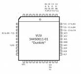
So as to get further with the diagnosis I'll either need a schematic of the card or at the very least the pin-out and functionality of the custom VLSI "Dunkirk" chip. Does anyone have either of these?

If in any doubt, I've attached an image of the board (before chip replacement).
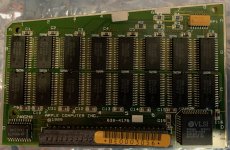
IMG_1800.jpg


Stephen_Usher

Well-known member
P.S. Just checked with all the SE/30 images on-line. No, it's not any of the chips on the SE/30. The closest part number is the Glue, but that's the wrong size and obviously designed before this chip as it's model number is smaller.


Stephen_Usher

Well-known member
I've been buzzing out some of the connections.

So far I've found the connections to A17-A23, LDS, VCC and GND on the input. So far, six output to pairs of CS- lines to the SRAM and the line to pin 11 (input 7) of the 74AC240 on the other side of the card.

I'm guessing that I could replicate the chip select (CS- line) decoding using a 74xx154 to decode four of the address lines to the chip selection. Having said that, at least one chip pair is getting selected all the time so I'd have to disable that somehow.


Stephen_Usher

Well-known member
With regards to chip select replacement I'm pretty sure that a 74HC154 would do the trick, if I could find all the *CS lines.

A22 and A23 could go through diodes and then both connect to the *E1 pin on the 154. A21 would go through an inverter to *E2. This would enable the output on the chip only if A21 is high and both A22 and A23 are low.

A17, A18, A19 and A20 would connect to the 154's A0, A1, A2 and A3 lines. The the *Y0-*Y15 outputs (active low) would go to the *CS pins of each pair of SRAM chips.

I'm hoping that all 16 *CS line do go appear on the VLSI chip as then a patch PCB could be connected to take over the chip select functionality.

 
Last edited by a moderator:

Stephen_Usher

Well-known member
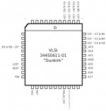
OK, found some more of the pin assignments:

Dunkirk-small.jpg

I've also powered the board separately and checked the voltages. Most of the pins on the "top half" of the chip, other than Pin 1, are at Vcc voltage whether or not A21 is high or not In fact nothing seems to change. None of the chip select lines are high either. This should mean that the board should be totally inactive when it's in the machine but it's obviously not as it wouldn't cause the chimes during the memory test.

The address range of this board does start at 1MB doesn't it?

 
Last edited by a moderator:

Trash80toHP_Mini

NIGHT STALKER
Nice detective work! I'm wondering if we can deduce the Dunkirk Operation. Given its fairly limited function, how complex can it really be?

ISTR mentions of silicon that can speak 5V and 3.3V depending. Between reverse engineering Dunkirk's ops and finding just that right controller, it might be possible to employ something like a "tiny" SODIMM or summat as MaxMem and possibly battery backed up RAM Disk of insane capacity in lieu of mass storage? Did something like that for the "System partition" of my maxed out PB100. Might have been RAMdisk+ that I used? Dunno, but in such a scenario the only time a Luggable would have to hit the horrid, SCSI bottleneck of SCSI2SD would be to reload contents of the RAM Disk.


techknight

Well-known member
@Maceffects is supposed to be releasing produced RAM cards for the portable, He has taken that project on to bring it to the market. 

Thats for new ones anyways. 

As far as yours, yea that VLSI is very specific for that card. its programmed to be a demultiplexer as well as a little bit of extra logic for DTACK and other. 

On my design, I use a 4 to 16 demultiplexor for MB barrier address decoding inside an XC9536.

Your card, you could possibly use an XC9536 to replace that chip with some patchwires, but you have to create the logic and program the chip. 

When working with the 68K, you need to decode the address bus and enable the chip select for the correct binary slices that each chip would fit within on the data bus. But not only that, the 68K has both an Upper, and Lower data strobe. So when working with even addresses the Upper strobe is asserted. Odd addresses, the Lower strobe is asserted. This is only valid for 8-bit transfers. But, a 16 bit transfer, both lines are asserted. 

This has to be taken into account to determine which block of chips are enabled for the given bus cycle, and this is part of the logic as well. To recreate the chips logic, you need to create a netlist and reverse-schematic based off that netlist from that particular RAM card. once You, I, We can stare at the circuit for a bit, I could whip up a quick functional logic block for that card to function properly. 

 
Last edited by a moderator:

techknight

Well-known member
Oh and to follow up:

Yes, the card's decode space starts 1MB above 0. or 0x100000h. 

since each chip is 32KB, that means the demux/decoder has to listen to address bits A15, A16, A17, A18, and A19. A20 enables the decode space for the entire card as thats between 1MB and 2MB. But to prevent Mirroring, A21, A22, and A23 are also monitored to insure the card ONLY decodes at 0b0001 

 
Last edited by a moderator:

Stephen_Usher

Well-known member
Thanks, that's what I thought, so for the address decode a 74LS240, an and-gate or two and a 74HC154 4 bit address demultiplexer would cover most of it.

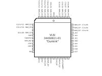
I've got a bit further today. I'm down to 6 pins I can't find the connections to, one of which should be the missing CS* line.

All the SRAM OE* and WE* lines common to all chips as are the two directional control lines on the two 74AC245 chips.

Dunkirk-small.jpg

 
Last edited by a moderator:

Stephen_Usher

Well-known member
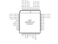
Yay! I've found the last RAM_CS* line!

Boo! I miscounted some pins and obviously bridged two of them iring testing.

Yay! I'm down to two mystery pins! :)

Dunkirk-small.jpg


Stephen_Usher

Well-known member
Well spotted. As it turns out one of the two mystery pins was A16 but the other was connected to pin 9 (O7) of the 74AC240 (G9), which has the input of pin 11 (I7), which is connected to SYS_POWER* (and hence the next pin to the left).


techknight

Well-known member
Then I wonder where A15 is going. I wonder if they designed the card to use A0 to A1, and A14 to A15. Decoding from A16 and above. 


Stephen_Usher

Well-known member
The initial checks of the two 74AC240s shows that they're being used purely as inverters for address lines A1-A15 and these are being passed on to the SRAM chips' A0-A14. _OE1 and _OE2 on both chips are tied to ground.

G9's I7 (pin 11) is being used to invert the SYS_PWR* line and feed it back to the VLSI chip.

So, the SRAMs are connected in pairs, it seems. One is the upper byte and one is the lower byte, both enabled by the shared _CS line. _OE is common for all chips but the upper and lower chips have separate _WE lines, probably controlled by the _UDS,  _LDS and _AS lines (note that there *IS* an _AS line on this version of the 68000 according to the Portable schematics, Pin 6).

 
Last edited by a moderator:
Top