Bolle
Well-known member
I've been working on recreating the IIfx logicboard on and off for quite a while.
Checking the date of creation of the schematics file it reaches back to September '21. I started by working my way through the BOMARC schematics and transcribing them into Eagle. Everyone who ever just looked at one of the BOMARC schematics knows how terrible they are to navigate through to find something.
I had a working board as well as a depopulated battery bombed board sitting next to me most of the time to compare against what's in the schematics or to fill gaps of things that did simply miss or didn't line up. That said, not blaming the poor soul who sat down and put those schematics down with just pen, paper, a multimeter and probably tons of datasheets for where they publicly existed back then which would mostly have been only standard chips.
The original IIfx board is a 6 layer board, with the majority of signals being routed on the internal layers, so it wasn't as "easy" as writing down what you see.
A few docs that @Arbee sent me later down the road did help verifying some of the custom chips pinouts and putting names to signals that just had placeholders.
With the schematics mostly done the project sat there for a good year and I didn't touch it until recently. After the sidequest of creating a LC475 board went through in two weeks I gained confidence that the IIfx can be done as well.
My own goal was to get it done on a 4 layer board instead of the original 6 layers they used back then.
On one hand to keep the costs down... (a 4 layer board of this size already cost me 180€ for a batch of 5 boards from JLC)
...on the other hand - well, because I can (probably I wasn't sure I could until I was halfway through)
After a day or to taking measurements and placing components ended up with some major ratsnest spaghetti:
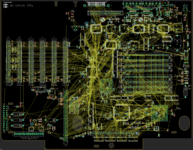
Going through the 24 stages of determining if it's going to be possible to route while staying within the 4 layer goal. It looks possible at first, then impossible after running the first traces, it then looks more and more possible just until you run into roadblock already and issue ripup; to start over.
Once you actually make it through routing the major address and data bus signals without blocking yourself out it's coming to the point to tell if there's enough space to fit everything and if the (random) choice of horizontal vs. vertical traces on the top or bottom layers was the right one.
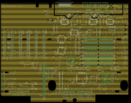
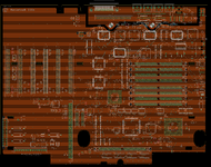
That's with Nubus, all three!!! data busses and the (not so critical regarding routing space because of the part layout) address busses laid down:
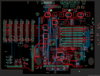
3552 airwires from 718 different signals connecting 563 components later...
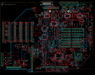
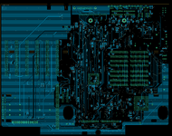
Prove I wasn't cheating myself - only power traces (-5V and a filtered 5V supply to the SCSI controller) running through the internal layer that's otherwise mostly a huge 5V plane:
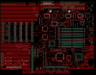
While we're at it babbling about power rails... the SCSI controller receives a filtered 5V rail that runs through a ferrite before it's passed to the chip.
On the original board Apple nicely placed decoupling caps close to all the relevant 5V pins on the SCSI controller - they just forgot to connect them to the correct power rail so they ended up doing nothing because power for the chip was actually drawn from the main 5V plane several centimeters away where the ferrite is located.
After at least two weeks of staring at the supposedly finished board and finding another error every other day I finally pulled the trigger and ordered some boards.
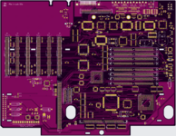
And because I had to wait and you're probably waiting to see the final result as well if you're still reading what's written that far down here's the opportunity to stare at the beautiful renders that I stared at for at least an hour a day while waiting for the boards to arrive:
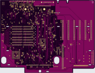
Once the boards were here everything went down really quick - as quick as possible at least. I was working extremely careful to make sure there's no soldering mistakes at all, otherwise troubleshooting would become a nightmare on this board. Even more so because nobody knows how they actually work and there's no known troubleshooting procedures out there except the good old "stare at it until it starts working" method that I'll obviously have to talk about later. (not because of a soldering error - there was none)
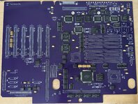
Here come the PCBs...
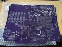
Only the cleanest donor parts I had around found their way onto this board. The two battery bombed donor boards did still death chime so I knew they weren't completely dead
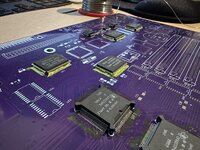
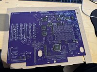
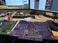
Did I mention there's 282 passives on the bottom of the board?
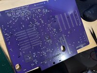
Moved them all over from the donors to ensure I have the correct values for all of them. Nothing worse than having to find that one resistor that is pulling a signal up with 100ohms where it should have been 10k ohm.
Finally reaching the state where it should have death chimed:
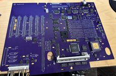
... and it actually did after messing around with the jumpers on the board. @zigzagjoe sent me one of his blinkenSIMMs and it proved really useful right from the start. The board was just sitting there idling with random data on the databus and an address on the address bus that didn't make any sense.
After fiddling with the jumpers on the board I did get a deathchime but only when the jumper to disable the 32k cache was set.
I worked my way through the (visible to me) logic that interacts with the cache, mostly the address decoder PAL at UL6 that generates the enable signal for the four cache chips and the cache tag. It didn't make sense at first because it seemingly enabled the cache right from the start where you'd expect the 68030 to walk the bus in order to find code to run from the ROM.
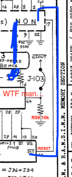
After a few days of staring at the board (here we are) I found that I missed to hook up the reset line on the cache tag chip to the main system reset:
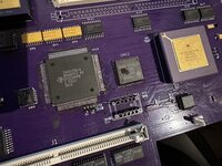
With that bodge in place the board did instantly chime (good chimes even without RAM, because everything up that this point seems to fit into the 32k of SRAM before it locks up)
Want to know how the Bomarc schematics indicate this should be hooked up to the main system reset? THEY FRIKKIN don't. Instead there's just a single line drawn to the parity generator. If they would have just let it out I would've investigated and noticed it while drawing the schematics.
After getting the happy chime I added the rest of the components, plugged in a video card and got no video output but I could see from the activity LED on the SD card adapter I had hooked up that it was booting.
That next mistake is actually on me... missed to connect the third Nubus slot ID bit to ground on all slots:
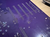
With that in place the board video came up, all slots work, SCSI, Floppy, Serial all the fancy IOP stuff in A/UX, everything just works.
I am still blown away that those two bodges was all it needed to get it working on a complex board like this with no proper schematics or documentation at all.
I'm incredibly proud of the final result:
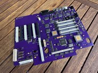
With all the unused space I added an ATX power connector as well as the necessary resistors and a transistor to invert /PFW to have soft-power just work without modifying the power supply at all. There's also a jumper next to the two HC132s that control powerup/-down to feed 5Vsb from an ATX power supply to the poweron circuit so you don't need the second battery for soft-power when running an ATX PSU.
Obligatory coin cell and 1/2AA footprints for the batteries as well as footprints for both PLCC and through hole RTCs are modifications to the original design as well.
Parts layout around the poweron circuit isn't 100% the same as on the original either because otherwise there wouldn't have been enough space to fit the RAM data traces through the area.
The bottom layout is quite different but most parts did stay in the same area where it made sense. If you should find yourself in the situation to populate a board and can't find some parts you might have to flip the board because some passives went from top to bottom and vice versa also due to space constraints.
I reverse engineered the 6 PALs found on the board along the way, JEDEC files for GAL replacements as well as the gerbers for the board on github:

 github.com
Checking the date of creation of the schematics file it reaches back to September '21. I started by working my way through the BOMARC schematics and transcribing them into Eagle. Everyone who ever just looked at one of the BOMARC schematics knows how terrible they are to navigate through to find something.
I had a working board as well as a depopulated battery bombed board sitting next to me most of the time to compare against what's in the schematics or to fill gaps of things that did simply miss or didn't line up. That said, not blaming the poor soul who sat down and put those schematics down with just pen, paper, a multimeter and probably tons of datasheets for where they publicly existed back then which would mostly have been only standard chips.
The original IIfx board is a 6 layer board, with the majority of signals being routed on the internal layers, so it wasn't as "easy" as writing down what you see.
A few docs that @Arbee sent me later down the road did help verifying some of the custom chips pinouts and putting names to signals that just had placeholders.
With the schematics mostly done the project sat there for a good year and I didn't touch it until recently. After the sidequest of creating a LC475 board went through in two weeks I gained confidence that the IIfx can be done as well.
My own goal was to get it done on a 4 layer board instead of the original 6 layers they used back then.
On one hand to keep the costs down... (a 4 layer board of this size already cost me 180€ for a batch of 5 boards from JLC)
...on the other hand - well, because I can (probably I wasn't sure I could until I was halfway through)
After a day or to taking measurements and placing components ended up with some major ratsnest spaghetti:

Going through the 24 stages of determining if it's going to be possible to route while staying within the 4 layer goal. It looks possible at first, then impossible after running the first traces, it then looks more and more possible just until you run into roadblock already and issue ripup; to start over.
Once you actually make it through routing the major address and data bus signals without blocking yourself out it's coming to the point to tell if there's enough space to fit everything and if the (random) choice of horizontal vs. vertical traces on the top or bottom layers was the right one.
That's with Nubus, all three!!! data busses and the (not so critical regarding routing space because of the part layout) address busses laid down:

3552 airwires from 718 different signals connecting 563 components later...

Prove I wasn't cheating myself - only power traces (-5V and a filtered 5V supply to the SCSI controller) running through the internal layer that's otherwise mostly a huge 5V plane:


While we're at it babbling about power rails... the SCSI controller receives a filtered 5V rail that runs through a ferrite before it's passed to the chip.
On the original board Apple nicely placed decoupling caps close to all the relevant 5V pins on the SCSI controller - they just forgot to connect them to the correct power rail so they ended up doing nothing because power for the chip was actually drawn from the main 5V plane several centimeters away where the ferrite is located.
After at least two weeks of staring at the supposedly finished board and finding another error every other day I finally pulled the trigger and ordered some boards.
And because I had to wait and you're probably waiting to see the final result as well if you're still reading what's written that far down here's the opportunity to stare at the beautiful renders that I stared at for at least an hour a day while waiting for the boards to arrive:


Once the boards were here everything went down really quick - as quick as possible at least. I was working extremely careful to make sure there's no soldering mistakes at all, otherwise troubleshooting would become a nightmare on this board. Even more so because nobody knows how they actually work and there's no known troubleshooting procedures out there except the good old "stare at it until it starts working" method that I'll obviously have to talk about later. (not because of a soldering error - there was none)
Here come the PCBs...

Only the cleanest donor parts I had around found their way onto this board. The two battery bombed donor boards did still death chime so I knew they weren't completely dead


Did I mention there's 282 passives on the bottom of the board?

Moved them all over from the donors to ensure I have the correct values for all of them. Nothing worse than having to find that one resistor that is pulling a signal up with 100ohms where it should have been 10k ohm.
Finally reaching the state where it should have death chimed:

... and it actually did after messing around with the jumpers on the board. @zigzagjoe sent me one of his blinkenSIMMs and it proved really useful right from the start. The board was just sitting there idling with random data on the databus and an address on the address bus that didn't make any sense.
After fiddling with the jumpers on the board I did get a deathchime but only when the jumper to disable the 32k cache was set.
I worked my way through the (visible to me) logic that interacts with the cache, mostly the address decoder PAL at UL6 that generates the enable signal for the four cache chips and the cache tag. It didn't make sense at first because it seemingly enabled the cache right from the start where you'd expect the 68030 to walk the bus in order to find code to run from the ROM.
After a few days of staring at the board (here we are) I found that I missed to hook up the reset line on the cache tag chip to the main system reset:

With that bodge in place the board did instantly chime (good chimes even without RAM, because everything up that this point seems to fit into the 32k of SRAM before it locks up)
Want to know how the Bomarc schematics indicate this should be hooked up to the main system reset? THEY FRIKKIN don't. Instead there's just a single line drawn to the parity generator. If they would have just let it out I would've investigated and noticed it while drawing the schematics.

After getting the happy chime I added the rest of the components, plugged in a video card and got no video output but I could see from the activity LED on the SD card adapter I had hooked up that it was booting.
That next mistake is actually on me... missed to connect the third Nubus slot ID bit to ground on all slots:

With that in place the board video came up, all slots work, SCSI, Floppy, Serial all the fancy IOP stuff in A/UX, everything just works.
I am still blown away that those two bodges was all it needed to get it working on a complex board like this with no proper schematics or documentation at all.
I'm incredibly proud of the final result:

With all the unused space I added an ATX power connector as well as the necessary resistors and a transistor to invert /PFW to have soft-power just work without modifying the power supply at all. There's also a jumper next to the two HC132s that control powerup/-down to feed 5Vsb from an ATX power supply to the poweron circuit so you don't need the second battery for soft-power when running an ATX PSU.
Obligatory coin cell and 1/2AA footprints for the batteries as well as footprints for both PLCC and through hole RTCs are modifications to the original design as well.
Parts layout around the poweron circuit isn't 100% the same as on the original either because otherwise there wouldn't have been enough space to fit the RAM data traces through the area.
The bottom layout is quite different but most parts did stay in the same area where it made sense. If you should find yourself in the situation to populate a board and can't find some parts you might have to flip the board because some passives went from top to bottom and vice versa also due to space constraints.
I reverse engineered the 6 PALs found on the board along the way, JEDEC files for GAL replacements as well as the gerbers for the board on github:
GitHub - TheRealBolle/IIfx: Recreation of the Macintosh IIfx logicboard
Recreation of the Macintosh IIfx logicboard. Contribute to TheRealBolle/IIfx development by creating an account on GitHub.
