• Updated 2023-07-12: Hello, Guest! Welcome back, and be sure to check out this follow-up post about our outage a week or so ago.

Daystar Macintosh II Adapter dissection

Bolle

Well-known member
As there was some interest in that trading post thread over here I thought we might gather some information on the Mac II and the Daystar adapter here.

One difference this adapter has compared to all other Daystar adapters is that it (besides going into the CPU socket) plugs into the MMU socket that's only found on the Mac II.

Reason for that is that most of the address bus of the logicboard is cascaded behind the MMU like shown in the MC68851 user manual:

View attachment 24504

For the accelerator to be able to access the whole logicboard bus it has to connect right to the physical address bus (behind the MMU) as well as to the logical address bus (between 020 and MMU).

The adapter itself looks pretty straight forward:
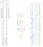
Daystar Mac II.png

All MMU control signals are disconnected as 030 and 040 upgrades don't need those because they have built in MMU features.

Most of the bus control signals connect straight through between the accelerator slot and the 020 socket.

There is a tiny 4096 byte PROM on the adapter (still gotta find a way to read it - it looks like my TL886 does not support the AM27S29 or any of the similar DIP20 512*8 ROMs.

Next to that we have a PAL20L8 that's doing address decoding to generate the chip select for the ROM - that's going to be easy once I find time to hook up the logic analyser.

The trickiest part is going to be the GAL16V8 that looks like it's generating address/data strobe signals to translate between the different busses (physical/logic on logicboard and accelerator)

Any takers for some guesses what the GAL might be doing exactly? *looking at @joethezombie*

 
Last edited by a moderator:

Bolle

Well-known member
BTW: The II flies with a 50MHz PowerCache. Did not yet try the Turbo040 but 40MHz 040 with 6 Nubus slots does sound like something everyone should have :D


Bolle

Well-known member
And the ROM on there:

Code:
aaaa55555800002e24436f7079726967 ..UUX...$Copyrig
68742031393931204461795374617220 ht.1991.DayStar.
4469676974616c2c20496e632e004e7a Digital,.Inc..Nz
00020280000020000080000008084e7b ..............N{
000241fa0008f01040004ed600000000 ..A.....@.N.....
00000000000000000000000000000000 ................
00000000000000000000000000000000 ................
00000000000000000000000000000000 ................
55aaaa5550f800aa500200020b564552 U..UP...P....VER
53494f4e20322e300452534620000452 SION.2.0.RSF...R
44472000044d4b4220000c3800010cb1 DG...MKB...8....
6634487a003621df002c11fc00030cb1 f4Hz.6!..,......
21fc408000500cb421fc000000400cb8 !.@..P..!....@..
42a7f01740002ebc58008607f0170c00 B...@...X.......
11fc0003012f59894ed12f002f08206f ...../Y.N././..o
000a20100c80f000400067280c80f01f ........@.g(....
4c006632f02f4c00001058883f6f000e L.f2./L...X.?o..
00162f4800123f6f00080010205f201f ../H..?o....._..
508f4e73f02f4000000458882f48000a P.Ns./@...X./H..
205f201f4e73205f201f2f3800304e75 ._..Ns._../8.0Nu
00000000000000000000000000000000 ................
00000000000000000000000000000000 ................
00000000000000000000000000000000 ................
00000000000000000000000000000000 ................
00000000000000000000000000000000 ................
00000000000000000000000000000000 ................
00000000000000000000000000000000 ................
00000000000000000000000000000000 ................
00000000000000000000000000000000 ................
00000000000000000000000000000000 ................
00000000000000000000000000000000 ................
00000000000000000000000000000000 ................


As always with rare gear you should take a soldering iron to it before even really using it :evil:

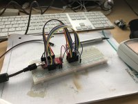
Reading the ROM was a bit of an adventure as those old small PROMs are not supported by my chinese ROM burner:

IMG_5958.JPG

 
Last edited by a moderator:

trag

Well-known member
Nice bench setup.   Do you do this kind of work for a living, because that looks like some very neat breadboard work.   And, of course, there are your adventures in G3/G4 swapping.  :)


Trash80toHP_Mini

NIGHT STALKER
Nice. I wonder if you could play some  extended MMU games on the Mac II at that wedge point? The on die 030 and 040 MMUs are but mere subsets of the great and powerful 68851. [}:)]


Bolle

Well-known member
Do you do this kind of work for a living
Not really. I studied communications engineering but my everyday job is only slightly related to anything electronics anymore ;)

For reading that ROM I simply hooked it up to an Arduino and wrote some code to cycle the address lines through all possible combinations and reading the data lines dumping the raw binary output to the console.

Next up I will hook up the analyser to the PROM and see when (or if at all?) it is used. I would imagine it patches something into the original ROMs early in the boot process. I wonder why if it even does anything as I already have the upgraded HD floppy ROMs in my Mac II (which should be identical to the IIx ROMs I think) and the IIx adapter does not have any logic on it and does not need any ROM patching at all to work with the PowerCache.

While the analyser is out I will see if I can figure out the address decoding PAL - shouldn't be too hard as it is combinatory - leaving the most fun part of the probably registered GAL as the final challenge.


Trash80toHP_Mini

NIGHT STALKER
I imagine the IIx ROM from the FDHD upgrade kit was a requirement for PowerCache in MacII. It was for the Rocket anyway. as was the PMMU. That's why I opted for a IIx, the guy I talked to at Sun Re- steered me right on course for smooth sailing  .  .  .  erm  .  .  .  liftoff?

Have we got the Mac II PowerCache installation instructions online here yet?


Bolle

Well-known member
Code:
chip u2 GAL16V8

CPUCLK=1 FC0=2 FC1=3 FC2=4 ROM_OE=5 AS_CACHE=6 DS_CACHE=7 BGACK=8 RESET=9 GND=10 /OE=11 f_DS=12 
AS=13 DS_CACHE=14 rf15=15 rf16=16 ro17=17 PAS=18 DSACK0=19 VCC=20 


equations

/DSACK0 = /AS_CACHE * /rf15
DSACK0.oe = /AS_CACHE * /rf15 * BGACK * RESET

/PAS = /FC2 * ROM_OE * /AS_CACHE
    + /FC1 * ROM_OE * /AS_CACHE
    + /FC0 * ROM_OE * /AS_CACHE
PAS.oe = BGACK * RESET

/ro17 := vcc
ro17.oe = OE

/rf16 := /ROM_OE * /AS_CACHE
rf16.oe = OE

/rf15 := /rf16
rf15.oe = OE

/DS_CACHE = /f_DS
DS_CACHE.oe = /BGACK

/AS = ROM_OE * /AS_CACHE
AS.oe = BGACK * RESET

/f_DS = ROM_OE * /DS_CACHE
f_DS.oe = BGACK * RESET


The DS pin is configured to use feedback.
 

The address decoder PAL for ROM_OE is next :evil:

Will have to hook up the analyzer to see where they mapped the ROM and when it is accessed.

 
Last edited by a moderator:
Top