Bolle, thank you. That is really helpful.Regarding the soft power problem: you have to place a jumper on either the ATX or the Mac setting next to the HC132s. (to match whatever power supply option you're using)
That's not going to solve your no chime issue though.
I'd start checking the usual... is everything coming out of reset? Does the CPU get a clock signal? (it looks suspiciously cold in that flir image)
Is the CPU walking the bus without a ROM installed?
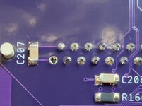
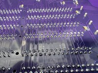
Check all solder joints again at least 10 times
Once you've got the board to chime a jumper should be installed at J103 to enable the external cache. J106 (forces the CPU to always operate at half clock speed) and J20 (disables internal CPU caches) should stay open.

I did not add any of the ATX items because I am using the stock power supply. But that would explain a lot.
I am getting no response when I press the reset buttons. Possible it is the Sony Sound IC's? The Audio out plug?
I did find a few pins that were not connected especially on those IC's with the small thin pins. I also had a few not connected on the PLCC type IC's. I checked again this morning and will recheck tomorrow. I think I am seven on my count of rechecking, so I have a lot more to go.
My donor boards are from two battery bombed boards. I have replaced some of the IC's that were damaged from the battery leakage. Like UC17 the Serial Communications Controller and UD16 which were both hit badly.
I also used all fresh resistors and capacitors when I prepped the board.
This is a great project of yours. I really appreciate being able to resurrect my damaged boards. I will continue to try to boot. I'm sure it's something that I missed.
Thanks for the response.