• Updated 2023-07-12: Hello, Guest! Welcome back, and be sure to check out this follow-up post about our outage a week or so ago.

LC PDS card design -- FC0/1/2?

dougg3

Well-known member
Hey everyone,

I've been experimenting with designing an LC PDS card that has a ROM SIMM socket on it in order to use the right half of the UI in Apple's Flasher app in my LC 475. Just for the fun of it! This has been an entertaining foray into programmable logic and is exactly what I needed for a simple starter project for understanding the 680x0 bus cycles.

I've been looking at the various LC series devnotes and also Designing Cards and Drivers for the Macintosh Family. One thing that is common to all of them when referring to the LC PDS slot is they all mention this or something similar:

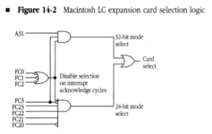
Your expansion card must generate its own card select signal. Figure 14-2 shows a typical example of the required logic. Notice that a function code of 111 (CPU space) disables the card select signal. This action is important because it prevents the card from being selected during interrupt acknowledge cycles.

It goes on to show a diagram of simple selection logic that makes sense. I don't think I've ever seen a NAND gate represented as an OR gate with all negated inputs before, but maybe there's a reason to show it that way (closer to what a PAL/GAL can actually implement?)
1703625883475.png

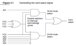
By the way, they made a typo and accidentally referred to A23 through A20 as FC23 through FC20. The LC 475 dev note shows it correctly:
1703626209030.png

Anyway, I'm ignoring the 24-bit mode selection logic for now because as far as I can tell, in the LC 475 I should only need to deal with 32-bit mode. It seems kind of silly to me that all of this logic would have to be replicated on every card, but I guess it makes sense because the original Mac LC didn't have an MMU so it couldn't easily remap 24-bit mode's 0xExxxxx to the corresponding 32-bit address space under the hood.

I'm not sure why the LC 475 devnote even mentions the 24-bit stuff -- maybe just for compatibility reasons with older Macs (would you ever see a bus cycle with FC3 = 0 in the LC 475?)

Now for the real reason I made this thread: I'm confused about something. And I'm hoping that someone with more experience might be able to help me understand what I'm missing. All of the info they say about making sure FC0 through FC2 isn't 111 makes sense to me. But with that in mind, why is it that I can't find FC0, FC1, and FC2 going anywhere on my Apple Ethernet LC Twisted Pair card? I thought for sure I'd see it going into the GAL on the card or something. But it seems like Apple didn't follow their own advice. I don't see any of those 3 signals going anywhere on the board. I've probed all over the place with my multimeter. I see plenty of other signals that make sense hooked up to the GAL: /AS, A31, FC3 (the 32-bit mode bit), /DSACK1, and the /OE pin of the card's onboard ROM.

Farallon's EtherMac LC NSC card does bring FC0-FC2 into the big ASIC on that card. So at least I know I'm not going crazy and other cards do pay attention to them...

How was Apple able to get away with ignoring FC0-FC2 on their card? The only thing that jumps to mind is that maybe they were clever with the card's address mapping and their GAL is looking at A19 and A18 to determine if it's an interrupt acknowledge cycle instead? Because A19 and A18 do go into the GAL, and interrupt acknowledge cycles have A19-A16 = 1111. So as long as all legit accesses to the card have A19 or A18 = 0, it could use that as the rule instead...

Thank you for any insight! I thought I was understanding everything and then this Apple card kind of threw me a curveball.
 
Last edited:

dougg3

Well-known member
I'm not sure why the LC 475 devnote even mentions the 24-bit stuff -- maybe just for compatibility reasons with older Macs (would you ever see a bus cycle with FC3 = 0 in the LC 475?)

Apparently I'm an idiot and the LC 475 does support 24-bit addressing, so nevermind on that!
 

dougg3

Well-known member
The only thing that jumps to mind is that maybe they were clever with the card's address mapping and their GAL is looking at A19 and A18 to determine if it's an interrupt acknowledge cycle instead? Because A19 and A18 do go into the GAL, and interrupt acknowledge cycles have A19-A16 = 1111. So as long as all legit accesses to the card have A19 or A18 = 0, it could use that as the rule instead...

This doesn't appear to be what they did. If I try to dump memory at 0xE00C0000, which is in the PDS card's super slot space and has both A19 and A18 = 1, I read back data. I believe if the card behaved based on the guess I described above, I would get a bus error instead...

Edit: In fact, the data I read back at that address (and 0xE0080000, and other repetitions) is actually the content of the 341-0740 chip which seems to contain the DeclROM.
 
Last edited:

dougg3

Well-known member
So I played around some more with the various address bits, and it seems like if I try to do a read from any 0xExxxxxxx address with A24 = 1, the system hangs. And sure enough, A24 is one of the address pins that goes into the GAL.

This sounds slightly crazy, but I'm starting to wonder if maybe they simplified the logic on this card so that A24 = 1 means it's an interrupt acknowledge cycle and used that instead of FC0/FC1/FC2? Probably fits much easier into the GAL...
 

ymk

Well-known member
1703642141802.png

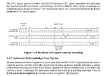
If your card has a small address space and can dodge the three FC==7 modes above on address alone, then you don't need FC.
 

dougg3

Well-known member
Thank you @ymk. That makes perfect sense. I've been studying the 68020 manual and now that you've pointed it out, I see the 68020 manual has a similar diagram. It also has access level control as another CPU space cycle similar to the first two. Thank you for pointing out that page and providing some insight!

I think that fully explains what's going on with this card. Breakpoint acknowledge and coprocessor comm. are already guaranteed to be ignored because A31 through A20 would have to be 0, and some of those bits are guaranteed to be 1 during PDS accesses. I think this card is using A24 to detect interrupt acknowledge cycles. It's good to know that it can be detected that way if you don't need the full address space. That's a lot simpler to implement than looking at FC0-2.

I installed MacsBug, played around, and confirmed that with this Ethernet card installed, any accesses to the card space with A24 = 1 end up as a bus error (likely because it never responds with /DSACK0 or /DSACK1 and the 45-90 us timer expires). Now it all makes sense. Thank you!
 

Trash80toHP_Mini

NIGHT STALKER
Great thread, found it last night killing time at work.

If I'm reading this right, you can take that card, using a limited memory block offline by only yanking on A24? Might you be able to use the remaining memory space and card addressing mechanics to access a second, unrelated function on a card for the functional equivalent of two slots?
 

dougg3

Well-known member
I'm definitely not an expert at this stuff but you can definitely split the available address space of the LC PDS slot up into multiple sections used for different purposes. The Ethernet card I was looking at already kind of does this -- the DeclROM is mapped to one section of the address space and the Ethernet chip is mapped to another. I'm sure you could map multiple peripherals like this. I'm not sure what it would take to share the /SLOTIRQ signal between them if more than one thing needed an IRQ though.
 

Arbee

Well-known member
For IRQ sharing the main thing would be getting the drivers trying to handle the IRQ to cooperate. I'm not super familiar with how that works on the software end, but I assume only one thing can register to handle each interrupt so that would get interesting fast. Especially for video cards where the driver usually comes from ROM before the OS loads.
 

Melkhior

Well-known member
I assume only one thing can register to handle each interrupt
No, even in System 7 (didn't try older) you have multiple functions handling one interrupt. They need to check if it's "their" interrupt, if yes they handle it and say so, if not they ignore it and say so. If ignored, System 7 calls the next handler in the order of priority. NuBusFPGA uses it to share the interrupt between the framebuffer (required VBL interrupt used for e.g. the mouse) and the other driver such as the RAM disk.

However, as you mentioned, it requires the SW to behave nicely and confirm the interrupt is for them before handling. If a handler just assumes its "their" interrupt and react to the interrupt line unconditionally, then sharing won't work (unless you only have one of those and put all of the others are higher priority to work around the problem). It also the HW to provide some way to check if they did raise an interrupt or not for the handler to check - otherwise, again, sharing problem.
 

Trash80toHP_Mini

NIGHT STALKER
I've always been interested in what exactly the DCaD tomes mean by "further decoding" when it comes to expansion slots. This is the first instance that's come up where I might be able to beg a clue?

What I was thinking was that the second function would monitor A24. When the system yanks on it the NIC stays offline, so when it is yanked upon, I was thinking that FC0/1/2 or summat might be invoked to put the second function into play when its dedicated memory space is invoked?

Dunno, crazed, knuckle draggin' Neanderthaler here. This is so far above my pay grade it's laughable. But I do love poking around for chinks in the Macs armor with my fire hardened stick. 🤪
 

Melkhior

Well-known member
I've always been interested in what exactly the DCaD tomes mean by "further decoding" when it comes to expansion slots.🤪
To define "further decoding", the safest way is to start by defining "decoding" :) So here's a not-so-little primer on building a system based on the MC680[23]0, which I will shorten to '030 from now on. We will only consider physical addressing, as it's the one relevant for the question. And on Macs without virtual memory, virtual and physical addressing are very close to one another.

The '030 has what is called a "flat" address space. This means it doesn't differentiate between memory addresses; they are all equivalent from the point of view of the CPU. Their meaning is defined by the system designer - whomever is creating the actual computer using the CPU. Everything in the system (with a few exceptions to be discussed later) is addressed by the CPU via memory addresses. The software must know about the "meaning" to work properly and talk to the right piece of hardware.

The '030 has 32 address "lines", A0 to A31. So we have up to 2**32 (a.k.a. 2^32, 4,294,967,296) bytes addressable. Every device (including the memory controller, NuChip, VIA, etc.) is defined by the system designer has being "mapped" somewhere in the address space, that is, some of those bytes are defined as accessing a register or some memory in the device/memory controller/... That's the "address map" you have in various apple documents - you can find details in for instance "Guide to the Macintosh Family Hardware (2nd Ed)" page 34. The map for the SE/30 is on page 41, figure 1-26. For instance , the sound chip is at $5001_4000 (0x50014000 in modern hexadecimal), up to $5001_5FFF inclusive (SWIM starts at $5001_6000). That's often called the "memory space" for the device.

And that's where the first decoding step happens: the '030 has a 32-bits (4 bytes) bus, not a 8-bits (1 byte) bus. So A0 and A1 are "special". So for decoding, that would practically be the "last" step is to check for the byte address:
  1. Am I the device the CPU is talking to?
  2. Where is the byte or bytes the CPU is talking to ?
To check for (1), in theory, one should check whether the address is one of the 8192 ($2000 == 8192) possible bytes. Practically, the SE/30 will not bother: the address map is defined in a "smart" way, so that only *some* of the bits need checking. $5001_4xxx (binary: 'b0101_0000_0000_0001_0100_xxxx_xxxx_xxxx) and $5001_5xxx ('b0101_0000_0000_0001_0101_xxxx_xxxx_xxxx) are enough to check. In fact, when we look at the binary, we don't need to check the thirteenth bit from the right - we're in the device whether it's 0 or 1. So the system can simply look at A13 to A31 (19 lines) and compare it to 'b0101_0000_0000_0001_010 (19 bits) and ignore the lower 13 bits. That tekll us "I am the device the CPU is talking to".

For the byte or bytes, the device need two information: size and position. Those are supplied by A0 and A1 for position, and by two extra signals SIZ0 and SIZ1 for size. There's some magic in the bus protocol for devices narrower than 32-bits, I won't go into detail, so we can say the procedure for the example of the SE/30 sound chip as:
  1. Am I the device the CPU is talking to? => check A13 to A31 for the right address
  2. Where is the byte or bytes the CPU is talking to ? => check A0, A1, SIZ0 and SIZ1
Of course, that's nowhere near enough for the sound chip to work (or any other device/memory controller/...). It needs to know what specific address the CPU is talking to - a control register, some buffer memory in the chip, ... So what the chip really needs is:
  1. Am I the device the CPU is talking to? => check A13 to A31 for the right address (in my memory space)
  2. Which register/memory is the CPU talking to ? => check A2 to A12 inclusive for the 2048 possible 32-bits word available in my memory space
  3. Where is the byte or bytes the CPU is talking to ? => check A0, A1, SIZ0 and SIZ1
That's what "decoding" is, conceptually. But in real life, peripherals chip don't connect to all those address lines directly - it wouldn't make sense. First it doesn't know where it should be - and you don't want it to, as you may need more than one. The SE/30 has two SCC chip, one at $5000_0000, one at $5000_2000, so an external mechanism must be used. Second that's too expensive (many pins) and CPU-specific. So the device itself has a lot fewer pins:
  1. Am I the device the CPU is talking to? => one single dedicated pin (often "Chip Enable", "Chip Select" or similar)
  2. Which register/memory is the CPU talking to ? => a small number of pins, sufficient to address all the internal hardware, for instance 7 pins if 128 "things" inside the device
  3. Where is the byte or bytes the CPU is talking to ? => usually the device fixes the width so doesn't care, external hardware will deal with that
And a different chip, an external "decoder chip", handle the actual decoding of addresses, so you would have the following for a 32-bits device:
  1. A13 to A31 are connected to the decoder chip, producing a single "Chip Enable" signal for the device
  2. A2 to A8 are connected directly to the device addressing pins (in the 7-pins example)
  3. A9 to A12 are often ignored in that 7-pins example ! (more below)
  4. A0, A1, SIZ0, SIZ1 are connected to the decoder chip, which will do the required magic on the bus to "match" the CPU expectations and the device behavior
The "fun" thing is that point (2) and (3) are a bit more versatile - you could connect a different subset of address lines to the device, it would simply change the address at which the device internal stuff will "appear to be" to the CPU. Apple is actually doing exactly that for the SCC chip, so that the "lower" address lines (A2, A3, ...) don't have too much stuff connected to them. In the SCC, the first register is at $5000_0000, but the second one is at $5000_0200 if memory serve, rather than at $5000_0001 where you would expect it (one 8-bits byte later, the SCC is 8-bits).

You can also ignore some address lines. The device will behave the same no matter their value. It wastes address space, but it simplifies decoding because you don't need to check too many bits per device, and the decoder chip can have the same specifications for multiple devices. You just allocate an "address space" big enough for any one device to all device, and waste space when the device is "smaller".

In the SE/30, the "decoder chip" is the GLUE, and it does the job for all devices in the system - so it is connected to all the address lines, and it has a bunch of internal "comparators" and it outputs a lot of "Chip Enable"s (plus the required stuff to deal with the bus protocol itself, but that's out of scope).

For now, we have ignored the FC0, FC1 and FC2 signals that are the subject of this thread... but we need to address them. Whenever the CPU is using the bus (for read or write), it also indicates over FC0..2 what is the source of the access: user instruction, user data, supervisor (operating system) instruction, supervisor data. Practically, no-one cares for any of those! There's just one that is meaningful: when FC0..1 is all-one, then the CPU is NOT doing a memory access. It's basically ignoring the whole "flat memory" and "memory map" stuff and saying, "whatever you see on A0 to A31 is NOT an address, please ignore it unless you're my special friend who knows the special handshake". Among those special friends you will find the MC68881 and MC68882 FPU, the MC68851MMU (for the MC68020), and some handling of interrupts. Generally speaking, for any device, it just means that the "Chip Enable" signal doesn't just check the address, it must also check that FC0..2 isn't 'b111. That's it. But adding a whole lot of hardware just for that is expensive :-(

So now we can move on the "further decoding" bit :) The expression appear in DCDMF3 table 15-15 p361 for the IIsi:

RBV An active-low chip-select signal for the RAM-based video IC.
This signal can be used, along with further decoding, to enable
signals for a cache circuit.

chip-select == "Chip Enable", it's basically a signal saying "the address currently on the bus is in the area the system reserves for the internal video", which is $5002_6000 to $5002_7FFF (DCDMF3 p344). It's not actually needed - the IIsi has all the address lines on the PDS slot, so it's possible to recreate the signal by comparing the upper 19 bits to $$5002_[67]xxx and recreate the signal. But Apple supplies it so PDS device can save hardware and avoid adding more stuff connected to the address lines (having too much stuff on the same line will cause signal quality issue).

The idea of "further decoding" is just that *some* of the steps are already done, but the specific device might need more. For instance, if you look at a NuBus device:
  1. The GLUE (or equivalent) will check if the address is in the NuBus reserved range, from $6000_0000 to $FFFF_FFFF inclusive. This produces a "NuBus" signal available on the PDS, and this signal tells a NuChip (if present) to handle the request.
  2. A PDS device will need to decode further if it's more specifically in the slot or super-slot area reserved for the PDS - so in a IIsi, it check the upper bytes (A24 to A31) is $F9 for the slot, or it checks the upper nybble (half bytes, 4 bits, A28 to A31) is $9.
  3. A NuBus device will need to decode further from the request re-emitted by the NuChip if it's more specifically in the slot or super-slot area reserved for this particular slot. So it check the upper bytes (A24 to A31) is $F<ID0..3> for the slot, or it checks the upper nybble (half bytes, 4 bits, A28 to A31) is $<ID0..3>, where ID0..3 are the 4 ID lines on the NuBus slot.
  4. Then if you have multiple "things" on the PDS/NuBus device, it will need to decode further which specific bits is being addressed. As a for instance, @halkyardo SEthernet/30 checks whether you're reading from the ROM or reading/writing to the Ethernet chip by checking A16. So the CPLD implementing the "Decoder Chip" is connected to A24-A31 for the "is it me" check, and A16 for the "ethernet or rom" check.
  5. Then the relevant chip will have access to some of the address lines to decode which exact register/memory to use. For the same SEthernet/30 example, the Flash-playing-the-ROM is connected to A0 to A15 to expose 64 KiBytes (it's only 8-bits wide so it needs A0 and A1 connected to it directly). The Ethernet device is connected to A1 to A14, and it exposes 16384 (2**14) 16-bits words (it's a 16-bits wide device, to it needs A1 but not A0...), or 32 KiB.
So whenever the '030 talks to a SEthernet/30 in a SE/30 or IIsi, then it talks somewhere in the $F9xx_xxxx range, and:
  • If A16 is 1, it's the ROM, so $F901_xxxx is somewhere in the ROM. However, because the CPLD doesn't bother looking at A17 to A23, $F9FF_xxxx will read the same byte - and it's a feature not a bug because that second one is where the Slot Manager will actually look for the ROM! And that same byte is also visible at $F977_xxxx, $F915_xxxx, etc. As long as the two bytes after $F9 are "odd" (A16 == 1), it's the ROM, which bytes is from the $xxxx.
  • If A16 is 0, it's Ethernet. So $F900_0xxy ('y' must be even, not odd, because 16-bits) is somewhere in the Ethernet device. However, because the CPLD doesn't bother looking at A17 to A23, and because the Ethernet device doesn't bother looking at A15, then $F9A6_8xxy will read/write the same 16-bits word - those two bytes after $F9 are also ignored except for A16, and in addition A15 is ignored as well.
And that's why the LC PDS is a crappy design - it doesn't connect all the upper 8 bits A24 to A31. So you can't check the most important bits when decoding, as those are almost always needed to make sure you're in the "right" device. You're limited to implementing something in the area where the pre-decoded "slot" signal (a "Chip Enable" for the whole slot) is active, has handled by the "decoder chip" in the LC motherboard.

Another important point, more relevant to this thread, is that often you don't need to decode everything. As long as you decode "enough" to guarantee no other device will react, then it can be OK, provided the software doesn't scr*w up. Hence the "optimizations" discussed earlier, where some device takes shortcuts because they know how the rest of the system will behave... So in that instance, rather than expensive hardware to check whether FC0..FC2 is 'b111, they figure out what the "special handshake" to the "special friends" (FPU cycle, interupts acknowledge, ...) that can practically (in this specific system) happen look like, and make sure they never react to any of them. The trick is to use a small subset of the available "address space" whose valid address patterns never overlap with the "special handshake" patterns, and you can potentially avoid quite a bit of hardware... It's ugly but it's a clever way to save a bit of money.
 
Last edited:

Arbee

Well-known member
@Mehlkior I think you meant "VIA" instead of "SCC". Or at least that's what's at $50000000 and $50002000 in most NuBus machines. That's just a tiny nitpick though, the explanation itself is fantastic.
 

Melkhior

Well-known member
@Mehlkior I think you meant "VIA" instead of "SCC". Or at least that's what's at $50000000 and $50002000 in most NuBus machines. That's just a tiny nitpick though, the explanation itself is fantastic.
You are of course absolutely correct, there's two VIAs there, the single SCC is at $5000_4000. Too late to edit though :-(
 
Top