• Updated 2023-07-12: Hello, Guest! Welcome back, and be sure to check out this follow-up post about our outage a week or so ago.

Macintosh SE/30 logicboard recreation (thread revival)

Bolle

Well-known member
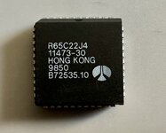
The use of the /Nubus signal in the video PAL is actually redundant. The video subsystem has its own address decoder… the LS30 decodes for slot E and F addresses, the PAL itself has A24 present to use the output from the LS30 to identify slot E accesses.
The /Nubus input could actually be removed from the PAL equations and everything would still just work.

The address decoder for the ethernet portion of my adapter card doesn’t use /Nubus for decoding the address, however the decoding logic I implemented to detect video accesses for the Carrera workaround uses /Nubus. That only matters if you want to run a Carrera though.
 

croissantking

Well-known member
The use of the /Nubus signal in the video PAL is actually redundant. The video subsystem has its own address decoder… the LS30 decodes for slot E and F addresses, the PAL itself has A24 present to use the output from the LS30 to identify slot E accesses.
The /Nubus input could actually be removed from the PAL equations and everything would still just work.
At the moment, with this line disconnected, you get a simasimac display but the machine works as normal - similar to if you try to boot up without a Video ROM inserted.

What you say about editing the PAL equations is interesting, because if you removed the /Nubus input you’d presumably remove the source of the interference too.

The address decoder for the ethernet portion of my adapter card doesn’t use /Nubus for decoding the address, however the decoding logic I implemented to detect video accesses for the Carrera workaround uses /Nubus. That only matters if you want to run a Carrera though.
I was just about to ask you about this - whether the Carrera 040 needs the Nubus line. So it plain won’t function with that line disconnected?
 

croissantking

Well-known member
EDIT2: if it works with the bodge wire and no PDS, but fails when you add a PDS card, you could try with a weak pull-down on the line (a resistor between ground and the /NUBUS). Something like 10kohm at first, and if it doesn't help be bold and go down to 4.8kohm. Going lower is also possible, but might entually overwhelm the drivers and force the signal low (active) all the time which doesn't help you. If the pull-down helps, then you know that there's some form of 'leak' between +5V (or a often-high signal) and the /NUBUS line.

I've just ordered these resistors, and am ready to do some experimenting.

Can I just double-check that I should be pulling the line low, rather than high? Is it a fair assumption that the interference is caused by something keeping the line high when it should be low, rather than the other way around? Because in my mind, the problem would more likely be that the line is active (low) when it shouldn't be.

IIRC, that recreated board is two layers only so it's not an issue with an internal layer...

It's a four layer board, but as I understand the internal layers are a ground plane and VCC.
 

bigmessowires

Well-known member
Reading back here a little, it sounds like @croissantking consistently saw the problem disappear when touching a metal probe to /NUBUS. Then they later tried to replicate this effect by adding a 10uF capacitor to /NUBUS, but it caused the video to fail completely.

I'd suggest trying again with a smaller capacitance value - 10uF is actually quite a large value and is much more than you're probably adding with your body and a wire probe. Try buying a set of ceramic capacitors with a range of values, then start with a value like 10 pF (one millionth of the value you used), and then work your way up by powers of 10 until the observed behavior changes.

But there's another puzzle here: why /NUBUS should affect anything. @Bolle says the /NUBUS output is a signal to indicate a memory access in a particular address range, but that it's redundant and unnecessary. If that's correct then theoretically it shouldn't matter if the /NUBUS value is correct or incorrect or present at all. So either you are chasing the wrong problem, or there's some secondary analog-level effect at work here.

Any fast-switching signal on a circuit board with sharp rising and falling edges has the potential to cause problems elsewhere. Maybe that's what /NUBUS is doing? It may be causing a ground bounce effect on the chip or another nearby chip, which you could try addressing by adding more decoupling capacitors with values between 0.01uF and 1uF roughly.

Sharp signal edges can also cause small glitches on adjacent traces on the PCB. Adding a small amount of capacitance to the rising/falling signal would round the edges a little bit and help reduce this type of interference. But if you add too much capacitance, the rise/fall times of the signal will become so slow that the circuit stops working.

As an alternative to adding capacitance, you can also add a small series resistor between the signal output pin and the trace. Try values in the tens of ohms range.
 

ThisDoesNotCompute

Active member
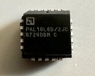
I have a question related to a couple of the PLCC chips.

Would this one be a suitable replacement for UH7?
uh7.jpg

And likewise, would this work for UK11 and UK12?
uk11-uk12.jpg

Thanks!
 

Bolle

Well-known member
But there's another puzzle here: why /NUBUS should affect anything. @Bolle says the /NUBUS output is a signal to indicate a memory access in a particular address range, but that it's redundant and unnecessary. If that's correct then theoretically it shouldn't matter if the /NUBUS value is correct or incorrect or present at all. So either you are chasing the wrong problem, or there's some secondary analog-level effect at work here.
Just quickly tested this on one of my boards by lifting the /NUBUS trace on the PAL and tying it to ground... unfortunately the board death chimes that way so it looks like it is needed - I don't see why because technically it is redundant but I also don't understand the video state machine enough to tell for certain. Timing differences between the decoder that's part of the video logic and the decoder in the GLUE could play a role as well.

Can I just double-check that I should be pulling the line low, rather than high?
Try both. On a "healthy" board it doesn't hurt the onboard video either way. Just tried by adding 10k towards ground as well as towards VCC.

It's a four layer board, but as I understand the internal layers are a ground plane and VCC.
Correct. Only a hand full of very short signal traces are running through one of the inner layers because there simply wasn't any space to route them on one of the outer layers (at least not economically)
The original design was using 6 layers: signal-VCC/GND-signal-signal-VCC/GND-signal, so each signal layer had only one adjacent reference layer just like on the 4 layer design. I don't really see how it could be an issue with noise or capacity on the signal... why would it just affect one single signal that's driven by the GLUE?
Bildschirmfoto 2023-11-24 um 20.04.15.png

I was just about to ask you about this - whether the Carrera 040 needs the Nubus line. So it plain won’t function with that line disconnected?
Correct again - at least with the way the adapter currently works.

Would this one be a suitable replacement for UH7?
Probably, but make sure you actually are able to program that one. (and pray it isn't already programmed because you can't erase PALs)
Just get a GAL or ATF... easier to get and you're on the safe side with them - plus you don't have to convert the JEDEC files on github as those are made for 16V8 devices and not 16R* or 16L* types.

And likewise, would this work for UK11 and UK12?
Looks like it should.
 
Last edited:

ThisDoesNotCompute

Active member
Probably, but make sure you actually are able to program that one. (and pray it isn't already programmed because you can't erase PALs)
Just get a GAL or ATF... easier to get and you're on the safe side with them - plus you don't have to convert the JEDEC files on github as those are made for 16V8 devices and not 16R* or 16L* types.
Thanks! I was able to salvage the original chip from the donor board, so I'll just clean it up and transplant it.
 

croissantking

Well-known member
Taking into account the advice from @Melkhior , @bigmessowires and @Bolle , I'm preparing to individually try the following tests:

- Tie the /Nubus line to GND with ceramic capacitors ranging from 10pF to 1uF in powers of ten and observe graphical interference patterns.

- Ditto, but tying to +5V

- Tie the /Nubus line to GND with 10K and 4.7K resistors and observe graphical interference patterns.

- Ditto, but tying to +5V

- Add a series resistor in the 10s of Ω range between the /Nubus output on the GLUE logic chip and the trace.


For the pull down/pull up tests, I'm planning to do this at the PDS slot as it's very easy to stick one end of the resistor/capacitor into the /Nubus pin, and another into +5V or GND.

Would it be a good strategy to try both a resistor and a capacitor at the same time, once I've worked out the most favoured values in each case?
 
Last edited:

croissantking

Well-known member
A couple more thoughts:

But there's another puzzle here: why /NUBUS should affect anything. @Bolle says the /NUBUS output is a signal to indicate a memory access in a particular address range, but that it's redundant and unnecessary. If that's correct then theoretically it shouldn't matter if the /NUBUS value is correct or incorrect or present at all.
@Bolle later went on to say that they had tried lifting the /Nubus trace from the PAL and got a death chime, and that it looks like it's needed.

So either you are chasing the wrong problem, or there's some secondary analog-level effect at work here.
My current thinking is that the interference isn't being caused by anything on the trace itself. Otherwise, my fix with the bodge wire wouldn't fall down with the PDS card installed. It seems to me as if the GLUE chip is outputting the interference. Maybe something else connected to the GLUE is messing with one of its inputs.

But yes, I agree it is possible that I'm looking in the wrong place. It's a good starting point though.
 

bigmessowires

Well-known member
My current thinking is that the interference isn't being caused by anything on the trace itself. Otherwise, my fix with the bodge wire wouldn't fall down with the PDS card installed.
What happens when a PDS card is installed, does the original problem with video corruption reappear, or is it a different symptom?

For tests of adding a capacitor, I don't think it matters much whether the capacitor is connected to +5V or GND.
 

croissantking

Well-known member
What happens when a PDS card is installed, does the original problem with video corruption reappear, or is it a different symptom?
The same symptom, but a different pattern [in terms of when it shows up, and intensity]. It looks like intense artifacting for about a minute (just long enough to boot up) and then everything suddenly goes away.

I found another interesting thing, which may or may not be important but I had some of the pick and place capacitors off for testing last night and the parts which should be 33pF are 10pF parts. Is this a reasonable substitution?

IMG_4727.jpg
 
Last edited:

bigmessowires

Well-known member
I'd be surprised if a 33pF part were actually 11pF unless the wrong part were used. If you clean the capacitor's pads really well, and also clean the tester pads, and push down on the capacitor body during testing to help ensure a solid electrical contact, does the value change?

Of course there's nothing magic about powers of 10 values, that was just a suggestion to help get through the range of possible values quickly. 33 or 11 or 10 are all fine for experimentation. If you're able to find a capacitor value that resolves your problems, my hunch is it'll probably be something between 10 and 1000 pF.
 

croissantking

Well-known member
I'd be surprised if a 33pF part were actually 11pF unless the wrong part were used. If you clean the capacitor's pads really well, and also clean the tester pads, and push down on the capacitor body during testing to help ensure a solid electrical contact, does the value change?
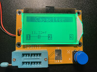
I’m pretty sure they’re part substitutions. I measured all 5 of the parts which should be 33pF and they consistently showed 11-12pF on my tester, pushing quite hard and also trying different positions. The other backside capacitors on my board so far seem correct, for example the one capacitor that should be 10pF also registers at 11pF, a 68pF one registers at 70pF, and so on. Testing the real 33pF parts from a donor board I have laying around show at 35pF on the tester.

Someone informed me that JLCPCB offers you part substitutions if they don’t have the particular component in stock. I didn’t order the Reloaded boards myself, so I wasn’t aware that this might have been done. There could be other backside components that are wrong, I’ll have to check everything now.

Of course there's nothing magic about powers of 10 values, that was just a suggestion to help get through the range of possible values quickly. 33 or 11 or 10 are all fine for experimentation. If you're able to find a capacitor value that resolves your problems, my hunch is it'll probably be something between 10 and 1000 pF.
Gotcha :)
 

bigmessowires

Well-known member
The original design was using 6 layers: signal-VCC/GND-signal-signal-VCC/GND-signal, so each signal layer had only one adjacent reference layer just like on the 4 layer design. I don't really see how it could be an issue with noise or capacity on the signal... why would it just affect one single signal that's driven by the GLUE?
Good question. You're right the problem might be something else entirely. I only suggested this explanation since it seems to fit the clues, especially the metal probe touching /NUBUS temporarily fixing the problem. And also because if the Reloaded PCB is identical to the original PCB from a schematic and netlist standpoint, and all the parts are the same too, then this would seem to be the only explanation left.

As for why it would only affect this one signal, I would suggest thinking of it differently. These kinds of problems with coupling and cross-talk are always there, on every PCB and on every trace. But most of the time they're small enough that they don't make any difference. The voltage on a trace can bounce and wiggle a little, and it won't disturb anything until the wiggle becomes large enough to fool another chip into thinking it's a clock edge, or to make a logical 0 briefly appear to be a logical 1.

If you wanted to intentionally force a problem like this to happen, you could make a long straight PCB trace, with a second PCB trace running directly next to it for a long distance. Then on the first trace, send a signal with a sharp rising or falling edge, and observe a faint echo on the second trace. Even better, have many parallel traces whose signals all rise or fall simultaneously, like you'd have with a data bus rapidly changing from 00000000 to 11111111. This will make the problem even more severe.

When I was designing the Yellowstone disk controller card for Apple II, I got stuck for a long time on a problem very similar to this. Whenever the card would change from driving 00000000 to driving 11111111 onto the 8-bit bus, it would cause terrible problems and often resulted in the computer crashing. You can see some of the oscilloscope captures here: https://www.bigmessowires.com/2021/06/19/yellowstone-glitch-part-6-this-is-getting-ridiciulous/ I eventually solved it two different ways. One was a firmware change to avoid changing too many output signals at the same instant. The other was the addition of small value series resistors in the signal traces, so the voltage changes would be less abrupt.

Of course this is all merely speculation unless we see some oscilloscope captures from an SE/30 Reloaded board. But my theory is there may be an issue like this with the /NUBUS signal, or a signal adjacent to /NUBUS, or a signal that's logically derived from it or that's used to derive it. And it's caused by minor-seeming differences in the way those signals are routed on the PCB, and it's not only /NUBUS that's affected but it's where the issue is severe enough to be noticed right now.

Another related possibility is that there's a design flaw in some combinatorial logic on the SE/30 board (you mentioned a PAL?), where it implicitly assumes that input signals will change in a particular order, else an output glitch may occur. Basically a combinatorial hazard. And on the original SE/30 board this requirement might be accidentally satisfied simply due to the PCB routing and differing parasitic capacitances on different traces, so that Apple's hardware designers never encountered it. But on a PCB with a different topology it might suddenly become an issue.

Adding a small amount of additional capacitance to a trace will slow down the signal, which might help. Adding a series resistor will have a similar effect, since the speed of signal change is related to the RC time constant. Adding a pull-up or pull-down resistor will bias the signal more towards 5V or GND, and may increase the signal switching time in one direction but decrease it in another. I probably wouldn't expect it to help with a problem like this, but it's worth trying.

Apologies for the long train of conjecture here, without much evidence to back it up. I'll be curious to see what can be learned from more testing. These kinds of problems can be maddeningly difficult to debug.
 

bigmessowires

Well-known member
Someone informed me that JLCPCB offers you part substitutions if they don’t have the particular component in stock. I didn’t order the Reloaded boards myself, so I wasn’t aware that this might have been done. There could be other backside components that are wrong, I’ll have to check everything now.
Do you have any idea what those capacitors are used for? 11pF instead of 33pF is a pretty significant difference and could cause some circuit malfunction. For capacitors in that value range, I'm guessing there are two of them paired with a crystal to create a clock oscillator?
 

croissantking

Well-known member
Good question. You're right the problem might be something else entirely. I only suggested this explanation since it seems to fit the clues, especially the metal probe touching /NUBUS temporarily fixing the problem. And also because if the Reloaded PCB is identical to the original PCB from a schematic and netlist standpoint, and all the parts are the same too, then this would seem to be the only explanation left.

As for why it would only affect this one signal, I would suggest thinking of it differently. These kinds of problems with coupling and cross-talk are always there, on every PCB and on every trace. But most of the time they're small enough that they don't make any difference. The voltage on a trace can bounce and wiggle a little, and it won't disturb anything until the wiggle becomes large enough to fool another chip into thinking it's a clock edge, or to make a logical 0 briefly appear to be a logical 1.

If you wanted to intentionally force a problem like this to happen, you could make a long straight PCB trace, with a second PCB trace running directly next to it for a long distance. Then on the first trace, send a signal with a sharp rising or falling edge, and observe a faint echo on the second trace. Even better, have many parallel traces whose signals all rise or fall simultaneously, like you'd have with a data bus rapidly changing from 00000000 to 11111111. This will make the problem even more severe.

When I was designing the Yellowstone disk controller card for Apple II, I got stuck for a long time on a problem very similar to this. Whenever the card would change from driving 00000000 to driving 11111111 onto the 8-bit bus, it would cause terrible problems and often resulted in the computer crashing. You can see some of the oscilloscope captures here: https://www.bigmessowires.com/2021/06/19/yellowstone-glitch-part-6-this-is-getting-ridiciulous/ I eventually solved it two different ways. One was a firmware change to avoid changing too many output signals at the same instant. The other was the addition of small value series resistors in the signal traces, so the voltage changes would be less abrupt.

Of course this is all merely speculation unless we see some oscilloscope captures from an SE/30 Reloaded board. But my theory is there may be an issue like this with the /NUBUS signal, or a signal adjacent to /NUBUS, or a signal that's logically derived from it or that's used to derive it. And it's caused by minor-seeming differences in the way those signals are routed on the PCB, and it's not only /NUBUS that's affected but it's where the issue is severe enough to be noticed right now.

Another related possibility is that there's a design flaw in some combinatorial logic on the SE/30 board (you mentioned a PAL?), where it implicitly assumes that input signals will change in a particular order, else an output glitch may occur. Basically a combinatorial hazard. And on the original SE/30 board this requirement might be accidentally satisfied simply due to the PCB routing and differing parasitic capacitances on different traces, so that Apple's hardware designers never encountered it. But on a PCB with a different topology it might suddenly become an issue.

Adding a small amount of additional capacitance to a trace will slow down the signal, which might help. Adding a series resistor will have a similar effect, since the speed of signal change is related to the RC time constant. Adding a pull-up or pull-down resistor will bias the signal more towards 5V or GND, and may increase the signal switching time in one direction but decrease it in another. I probably wouldn't expect it to help with a problem like this, but it's worth trying.

Apologies for the long train of conjecture here, without much evidence to back it up. I'll be curious to see what can be learned from more testing. These kinds of problems can be maddeningly difficult to debug.

Interesting to hear your ideas, I had a read through your blog entry, too. I'm definitely learning a lot as I try to debug this issue.

Do you have any idea what those capacitors are used for? 11pF instead of 33pF is a pretty significant difference and could cause some circuit malfunction. For capacitors in that value range, I'm guessing there are two of them paired with a crystal to create a clock oscillator?
Yes, three out of five of the 33pF parts are used in the Y1 and Y3 oscillator circuits. I believe another is used to tie an ADB (ADBF) pin to ground, and another to tie the floppy port 'write' pin to ground. Nothing directly related to the GLUE or to video.
 

croissantking

Well-known member
OK, I've found something interesting. The ASC generates the C16M clock signal that drives the PAL we have been investigating at UE7. And, on my boards, this same ASC has the Y3 oscillator and two incorrect capacitors fitted to its circuit.

I don't think I've mentioned it yet but touching the 'CK' pin on UE7 has made the interference worse when pressing on it with my finger. Basically the opposite effect to pressing on the /Nubus pin.
 

bigmessowires

Well-known member
If /NUBUS is expected to change slightly after the clock edge, but it's actually changing coincident with the clock edge or even slightly before (not sure if that's possible), then that would make sense. Touching the clock pin would slightly delay the clock and make the problem worse, touching the /NUBUS pin would slightly delay that signal and make the problem better. But I'm going to shut up now because I may be spreading a lot of FUD that's unrelated to the actual problem.
 
Top