• Updated 2023-07-12: Hello, Guest! Welcome back, and be sure to check out this follow-up post about our outage a week or so ago.

Apple prototype ROM flasher utility

SuperSVGA

Well-known member
Really? I haven't seen this. What machines have you seen this in?
It was available at least on the Portable, not sure how much earlier than that it was. The Portable for example would check for "SLIM ROM" at 0xE00000 and start code execution from 0xE00008 if found. There's also the checks for EDisk and Ginty ROM disks a bit later. I think some later sources mention "flash" ROM as well.
 

dougg3

Well-known member
What do think will be easiest, writing a new software that works similar to the linked one, but with support for modern chips, or trying to adapt this one?

For me, it probably depends on how far we need to go with software mods. I'm not sure if I'll actually have time to do much with this other than just hacking the software to the bare minimum needed to get it working. I think it would be fun to get this actual utility working just for the sake of being able to see what it was like. I guess another option would be to design a socketed clone of the Lobos board and program the chips in a standard ROM programmer like the XGecu T56. (My SIMM programmer can't do it because these chips need VPP and of course the /CS and /WE pinout doesn't match anyway)

Does the software probes the ROM at all, or rely on the Slot Manager to identify the Flash devices? Or does it assumes it's there if the user tells it so?

As far as I can tell, it's not doing anything with Slot Manager. When you first launch it, the software goes one by one through the big table of flash cards twice: once to identify if there's a SIMM installed, and once to identify if there's a PDS card installed. It's just blindly attempting write and read cycle combinations to put the chips into identification mode and read the manufacturer and product ID. If it finds matching manufacturer and product IDs, it knows something supported is installed. Also, when looking for a PDS card, it temporarily installs a custom bus error handler and attempts a read first. If the custom bus error handler executes, it knows the card isn't installed and moves onto the next entry in the table without ever attempting any write cycles.

Mapping the physical addresses to themselves shouldn't be needed

True, at least not for the slot addresses. The program's use of transparent translation is probably more important for handling the onboard ROM/ROM SIMM addresses. The Quadra ROMs only map a small amount of the available ROM space using the MMU, from 0x40800000 to the length of the ROM. But this software does write cycles to 0x40400000 (or 0x40200000 on the LC III), which wouldn't be mapped through the default MMU setup without using TT0. The only reason I'm familiar with this issue is because I had to help @Jockelill with reconfiguring the MMU tables in order to gain access to the full 8 MB of available ROM SIMM space for the ROM disk driver.

Using a NOT gate would mean you wouldn't need to hack the utility or worry about ROM accesses.

Ahh, I misunderstood what you were suggesting with the NOT gate. The way you have the NOT gates in the schematic you made (it's beautiful!) does make perfect sense if you want to keep both halves of the SIMM mapped at once. I was envisioning it more like a physical switch that chooses whether you're looking at the top or bottom half of the chips (pulldown resistor on the chip's highest address line, switch shorts it to 5V). The switch would just directly control the highest address lines of the chips. So with the solution I had been envisioning in my head, both halves wouldn't actually be mapped into the ROM space simultaneously. I think your solution is better, the only drawback being that it cuts the usable ROM space in half.

There's still a tiny bit of software support needed for your solution that keeps both halves mapped simultaneously, although it's a lot easier than the software support that would be needed for what I was thinking of. For your solution: if you're trying to program the half of the SIMM that you don't currently have selected (e.g. you're recovering from a bad flash), you have to change the addresses you're writing to accordingly. For example let's pretend it is a 2 MB SIMM containing two 1 MB halves. If you're booted from the lower half and trying to program the lower half, you want to write to 0x40800000. But if you're booted from the upper half (so it's currently mapped as the lower half) and you want to write the lower half (which is currently mapped as the upper half) you need to write to 0x40900000 instead. So the software doing the writing would have to be aware of that difference. Either way, this definitely sounds much easier than what I originally proposed about making sure you're executing from RAM and then asking the user to physically flip the switch on the SIMM.

It identifies my ROM as "read only" most likely due to the fact that it cannot regonize the chips.

Yes, that's correct. It's attempting write cycles and seeing if the chips respond as the various IDs that I listed above. You can confirm this by watching for brief low pulses on SIMM pin 3 with an oscilloscope when you open the flasher app. (Just be careful because 12V on pin 2 is right next to it!)

During my short testing I also did what one never should do, I took out the ROM simm and put in another one with whole system running!! My approach was, "what if I can insert another ROM and reprogram it", but the whole system hangs.

Eek! This is exactly what I was referring to when I was saying that my first "2 bank" solution would require software that gave the user time to flip the switch -- you can't flip away from the working ROM until you're sure you're not executing anything in ROM anymore. Also, that sounds incredibly dangerous to yank out the SIMM while it's powered! :)

I actually have a period flash ROM from a Apple Interactive TV system, but the problem is that as it is it will only boot in a Apple interactive TV system

Yeah -- if you had some way to externally program it with an actual LC 475 compatible ROM image, I'm confident it would show up correctly as a programmable SIMM in this software.

if your disk is full it tells you "disk full" and then you need to click on "Duh" :D. Don't say they didn't have humor.

Haha, yep! I noticed that. There are some other fun gems in there too. I haven't seen the message, but in the code if it can't open an image file it will say "Could not open image file" with a button of "Oh well".

I would think the PDS portion would just be for ROMs on PDS cards

I wish we had some examples of these cards somewhere. Sounds very interesting!

There's also the checks for EDisk and Ginty ROM disks a bit later.

I stumbled upon the Ginty stuff while disassembling the Color Classic ROM. There are also some interesting comments in the leaked source about this with V8/VISA based machines, where it looks for the ROM disk, then flips some bits in a register and tries again, then flips the bits back if it didn't find anything. The interesting comment there in the code is "we need to do this because we cannot tell if we have a PDS/PCMCIA flash card installed or a ROM exp. SIMM. With this bit cleared no DSACK is generated by the ASIC and with it set DSACK is generated by the PDS card attached." I wish I understood what was going on there...
 

SuperSVGA

Well-known member
There are also some interesting comments in the leaked source about this with V8/VISA based machines, where it looks for the ROM disk, then flips some bits in a register and tries again, then flips the bits back if it didn't find anything. The interesting comment there in the code is "we need to do this because we cannot tell if we have a PDS/PCMCIA flash card installed or a ROM exp. SIMM. With this bit cleared no DSACK is generated by the ASIC and with it set DSACK is generated by the PDS card attached." I wish I understood what was going on there...
The Data Strobe Acknowledge (/DSACK) is used to control the number of wait states. The processor asserts the Address Strobe (/AS) and the Data Strobe (/DS) to signal that the address is valid and data is ready to be placed on the bus (for reads) or has been placed on the bus (for writes). With /DSACK this ensures that enough setup time is available for devices to respond.

Typically the /DSACK signal would be asserted by either decoder/glue logic or interfaces, or another device on the bus.

What that note seems to imply is the ASIC on the board has a register that controls whether or not it asserts /DSACK for that address space. If it's just ROMs on the bus, they won't generate /DSACK on their own so the ASIC would have to do it. However if a more advanced device like a PDS SCSI card or something is installed, it may need to run faster or slower (e.g. with SCSI the transfer needs to complete) than the default /DSACK timings that would be acceptable for a ROM.

I can only assume that the default state is to allow the PDS card to generate the /DSACK. By enabling /DSACK generation it can check for the ROM, and turn it back off if there isn't a ROM there.
 

Bolle

Well-known member
While looking at it, I noticed that in the Q900, U30 (the PLCC controlling the Flash programming to the ROM socket, apparently) has an /OE signal (pin 16 of the PAL20R8D, presumably 28-pins PLCC) coming only from a testpoint. Doesn't that mean there will be the need for some 'external' intervention for the software to work?
Got a connection diagram for that PAL worked out already?

That's what it does:
Code:
chip U30 GAL20V8

CLK=1 i2=2 i3=3 i4=4 i5=5 i6=6 i7=7 i8=8 i9=9 i10=10 i11=11 GND=12
/OE=13 i14=14 rf15=15 rf16=16 ro17=17 rf18=18 rf19=19 rf20=20
rf21=21 ro22=22 VCC=24

@ues 5331353720202020
@ptd unused

equations

/ro22 := gnd
ro22.oe = OE
/rf21 := /rf21 * i7 * /i10
    + i7 * rf16 * /i10
rf21.oe = OE
/rf20 := /rf20 * i7 * /i11
    + i7 * rf16 * /i11
rf20.oe = OE
/rf19 := /rf19 * i7 * rf18
    + /i2 * i3 * /i4 * /i5 * i6 * i7 * rf18 * /i8 * /i9
rf19.oe = OE
/rf18 := /rf19 * i7 * rf18
rf18.oe = OE
/ro17 := i7 * /rf18
    + /rf19 * i7
    + /i2 * i3 * /i4 * /i5 * i6 * i7 * /i8 * /i9
ro17.oe = OE
/rf16 := i7 * /rf15
rf16.oe = OE
/rf15 := i7 * /i14
rf15.oe = OE
 

dougg3

Well-known member
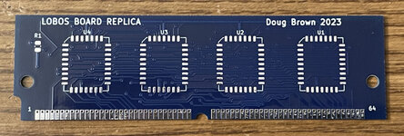
So...I did a thing this weekend and created a replica Lobos board in KiCad. My head is spinning, but I just finished matching up traces and vias to @Performa450's original pictures from this thread. I got a little lazy toward the end shoving things out of the way to make room for the last vias, and it's definitely not a perfect match, but it passes DRC! I'll probably order a few of these soon. Not sure I'll have much motivation to clean it up and turn it into an exact replica since it's just an experimental thing.

LobosReplicaTop.png
LobosReplicaBottom.png

I also ordered some Am28F020 chips on eBay, and I have an Xgecu T56 programmer (this wouldn't work with anybody's modern ROM SIMM programmers due to the chips needing 12V for VPP, not to mention pinout differences). I need to scrounge up some PLCC sockets, and then I should be able to build up a few of these and test out the flasher utility in a real Mac. We'll get to see exactly what it was like for Apple's ROM developers to reflash their Macs in-system during development!

This doesn't really have any practical applications -- it would make way more sense to hack the flasher utility to work with modern ROM SIMMs that use chips that are actually available these days. Or maybe make an entirely new program for in-system flashing instead. But I still wanted to do this so we can see the unmodified original flasher utility in action!
 

dougg3

Well-known member
Thanks Jockelill! I'll send one your way after I've tested it out. I cleaned it up a bit tonight and am just getting set up to order the PCBs. Yay! Can't wait to try out the flasher utility. I'll make a video of it in action, of course.

LobosReplicaFinalTop.png

LobosReplicaFinalBottom.png
 

dougg3

Well-known member
Lookie what showed up today. I'm excited to build one of these up and try it out with the Flasher utility! I have my Performa 630 all set up to attempt reflashing this SIMM in-system.

barepcb.jpg
 

Phipli

Well-known member
Lookie what showed up today. I'm excited to build one of these up and try it out with the Flasher utility! I have my Performa 630 all set up to attempt reflashing this SIMM in-system.

View attachment 65628
Excellent :) let us know how it goes. I'm very curious to see the projects this enables with 475s, 630s and 650s etc.
 

dougg3

Well-known member
Thanks Phipli and Jockelill!

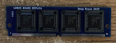
I have an update. I really need time to clean this up and present all this info in a nice organized manner on my blog and/or YouTube, but here's a sneak peek for 68kmla. The gist of it is: my Lobos SIMM replica works, and I was able to program it in my Performa 630 in-system using the Flasher app!

assembledpcb.jpg

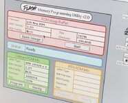
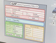
Here's what it looks like in the Flasher app with my replica SIMM installed. I programmed the four chips with the stock LC/Quadra/Performa 630 ROM using my T56 programmer to get things started. Notice that the program now detects a programmable "AMD 28F020 x 4" SIMM whereas previously it would say it was a Read-Only ROM. I also loaded a new ROM to flash with the "Open Image" button.

newromloaded.jpg

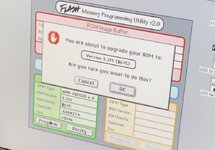
Then I clicked Program and it asked me to confirm:

areyousure.jpg

The actual programming process was pretty boring, which makes sense. It can't access anything in the Toolbox to display anything fancy, since that would be in the ROM that it's upgrading. So it just displays an "Upgrading..." message, which it probably draws before actually starting the process of erasing the chips.

upgrading.jpg

It looks like it's stuck and doing nothing, but it's really erasing and rewriting the flash chips behind the scenes. After about 10 seconds or so, I heard a boot chime even though this screen was still up. My "630 New ROM" file changed the boot chime, and that's what played, so at this point I was confident it succeeded!

The upgrading screen stayed up after the chime for a brief moment before it cleared and went forward with the normal boot process. When it booted back up, it warned me about shutting down uncleanly, which makes sense -- can't shut down cleanly if I'm upgrading the ROM.

All in all, great success! It definitely seems feasible to do the same thing this program does, but with newer chips that don't require VPP. Either by making a replica program, or hacking the code in this program. I still think hacking this program would be super cool because you would be using the same program that Apple's own developers used back in the day :cool: But I don't know if I would be biting off more than I can chew.
 

Jockelill

Well-known member
Really awesome!! Well done @dougg3 ! Can’t wait to play with this!!

Do you have a classic II machine? I remembered that I actually have some FPU boards with ROM provision for that machine. I would assume this software should also be able to program it?
 

dougg3

Well-known member
Thank you cheesestraws and Jockelill! It was super exciting to see it work on the first try.

Unfortunately I don't have a Classic II. This software doesn't support the Classic II though. It only supports the machines I listed in the first post in the thread, in addition to some other gestalt IDs which are mainly unreleased variants.

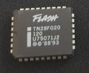
I notice at the top of the window it says this is version 2.0...I wonder what version 1.0 supported? Also, on a random note, I discovered that the "FLASH" logo in the window appears to have come from Intel's flash chips. Here's an image of one from an eBay listing:

1700804347695.png
 

Phipli

Well-known member
It only supports the machines I listed in the first post in the thread, in addition to some other gestalt IDs which are mainly unreleased variants.
Does the supported list change in the second version of the flash software we found?
 

tt

Well-known member
All in all, great success! It definitely seems feasible to do the same thing this program does, but with newer chips that don't require VPP. Either by making a replica program, or hacking the code in this program. I still think hacking this program would be super cool because you would be using the same program that Apple's own developers used back in the day :cool: But I don't know if I would be biting off more than I can chew.
Damn @dougg3 congrats on proving out the app with your Lobos replica!! It's interesting that you bootstrapped the ROM with the programmer and then were able to program it in-situ.

I am also interested in a board if you have any spares! It might be another unexpected use for my new Xgecu programmer. BTW, I used it recently to burn a new updated ROM for my Apple machine.
 

cheesestraws

Well-known member
The Classic II's ROM slot is weird. It's mapped in a different place in the address space to the OS ROM, so you can't use it to upgrade that, and it isn't in slot manager space either. Anyone know what it was actually intended for?
 

dougg3

Well-known member
Does the supported list change in the second version of the flash software we found?

I just spent some time staring at my disassembler looking into it. Here are the changes I found:
  • In the first version, I noticed there was a badly formatted table entry for the following gestalt IDs: 74, 75, 64, 65, 66, 100, 101, 111, 112, and 113. I don't think it would have worked because it was missing some entries. In the newer version this table entry looks more normal. I think these might correspond with the original NuBus Power Macs. 74 seems out of place, but maybe it was reused much later when the Power Mac 5400 came out.
  • Similarly, there was a badly formatted entry for these IDs in the first version: 116, 117, 118, 119, 120, 121, 122, 123. The newer version fixes this table entry too. These appear to correspond to various Quadras/Centrises with a Power Mac Upgrade Card installed (700, 900, 950, C610, C650, Q610, Q650, 800).
  • There's a brand new table entry for gestalt IDs 67, 68, and 69. This machine seems wildly different from the others -- for example ROM in this machine is at 0xFFC00000. This new flasher app version is called "Flasher (TNT 0.6)" so it makes sense that the 7500 would be included in this table entry. 67 = 9600, 68 = 7500, 69 = 8500. Not sure if these are completely accurate or if some of them were reused later.
  • The PowerBook Duo was split into different table entries. The 280/280c/gestalt 76 are treated separately from the other Duo models.
I'll have to try the newer version sometime. Wouldn't be surprised if there were some TNT-specific hacks in other places that make it incompatible though...

Damn @dougg3 congrats on proving out the app with your Lobos replica!! It's interesting that you bootstrapped the ROM with the programmer and then were able to program it in-situ.

Thanks tt! Yeah, bootstrapping with the programmer is a pain, but I don't think I had any other way. It's similar to what I had to do with my original IIci ROM hacking before the programmer existed. I definitely have a few spares. I'll earmark one for you!
 

Phipli

Well-known member
This new flasher app version is called "Flasher (TNT 0.6)" so it makes sense that the 7500 would be included in this table entry. 67 = 9600, 68 = 7500, 69 = 8500. Not sure if these are completely accurate or if some of them were reused later.
The 9500 and 9600 are both 67 - they didn't change the gestalt because they were so similar. 9500 would make sense as a first gen TNT based machine.

Would have expected to see the 7200.
 
Top