• Updated 2023-07-12: Hello, Guest! Welcome back, and be sure to check out this follow-up post about our outage a week or so ago.

Apple prototype ROM flasher utility

dougg3

Well-known member
I've been tinkering a lot with ROM SIMMs and Quadras lately. As a quick summary, most Quadras (maybe all of them?) seem to have been designed to work with a ROM SIMM. They generally have soldered ROMs and in most cases, especially on newer Quadras, the socket isn't populated.

@Performa450 shared pictures of this Lobos board ROM SIMM he bought a couple of years ago. I thought it was cool, and in that thread I even figured out that it was programmable and the programming voltage (VPP) and write enable (/WE) pins were brought out to the ROM SIMM socket (pins 2 and 3, respectively).

I didn't make the connection until recently when the @Jockelill started trying to get ROM disks working on Quadras, but the logic boards of the era seem to have 12V available for VPP on pin 2, and pin 3 is routed to whatever Apple ASIC is responsible for address mapping. I've physically confirmed this on my LC 475, Centris 610, Performa 630, and Quadra 660av. And it's becoming more and more clear that they're hooked up in general like this. What this means is...the Quadras were able to program their own ROM SIMMs in-system during development.

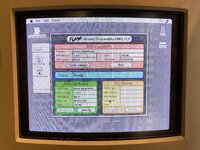
A couple of people have recently sent me a link to this Apple Flash ROM Utility on the Macintosh Garden. According to the description it came from a prototype PowerBook 520. I've been spending a bunch of time inspecting the code in this utility and disassembling it to understand it better. I've found several things that I thought would be interesting to discuss here, and I plan on updating this thread as I find more stuff.

It supports programming flashable ROMs in the following Macs. I'm listing them in separate groups just like how they're arranged in the code, to perhaps provide some extra context about what the unknown machine IDs might be similar to:
  • All of these 040 machines are grouped together, and also support flashable PDS cards:
    • Quadra 700, 900, and 950
    • Centris/Quadra 610/650, Quadra 800
    • LC 475/Quadra 605
    • LC 575
    • 630
    • 580
    • Unknown gestalt machine IDs 51, 57, 58, 59, 63, 86, 87, 90, 91, 93, 95, 96, and 97
      • A lot of these gestalt IDs appear to have been later repurposed for the Power Macs, but in this utility I'm pretty sure they represent older unreleased machines. There's a lot of 68k-specific code in the flashing routines for stuff like MMU config that I'm pretty sure wouldn't work in a PowerPC Mac.
  • The LC III is by itself with another unknown machine ID:
    • LC III (maybe an earlier prototype version that had a ROM SIMM socket?)
    • Unknown machine ID 40 -- seems to be another 030-based machine of some sort.
  • The AV machines are grouped together by themselves:
    • 660av/840av
    • Unknown machine IDs 43 and 79
  • These 030-based Macs are grouped together:
    • IIvx/IIvi/Performa 600
    • Unknown machine IDs 46, 47, and 55
  • PowerBook Duos are grouped together and in some cases have a ROM type referred to as "DBLite Flash":
    • PowerBook Duo 210, 230, 250, 270c, 280, 280c
    • Unknown machine IDs 39 and 76
  • More PowerBooks that use a "Dartanian Flash":
    • PowerBook 160
    • PowerBook 165c
    • PowerBook 180
      • The 180c is interestingly missing from this list...
  • These machines are grouped together and use a "Slice Flash":
    • Color Classic
    • Mac TV (again, no ROM SIMM...maybe an earlier board revision?)
  • Another group of machines that are similar to the above and also use "Slice Flash", but with a different ROM base address:
    • LC 520
    • LC 550
    • Unknown machine IDs 81 and 83
  • Final group that uses "Blackbird Flash" or "Malcolm Flash":
    • PowerBook 500
    • Unknown machine ID 73
This software is definitely going to be compatible with the Lobos board linked above. It seems to support various ROM modules that use the following chips and likely also works with the red programmable Interactive TV box ROMs I've seen:
  • Am28F020
    • It even seems to have support for a PDS card that has 16 of these chips onboard, which would result in a whopping 4 MB of ROM space
  • Am29F020A
  • Intel 28F020
  • Intel 28F010 (mistakenly identified by a string in the software as 28F256)
  • Intel 28F008SA
I've found the code that actually identifies, erases, and writes these chips. I'm still doing a bunch of research to understand it all. It looks like the unlock sequences and erase/programming commands are different between these flash chips and modern flash chips, so the utility would need to be hacked in order to work with newer stuff. I really think it would be cool to get this software working one way or another so we can experience what it was like to do ROM updates while working at Apple in the early '90s!
 

Phipli

Well-known member
Unknown gestalt machine IDs 51, 57, 58, 59, 63, 86, 87, 90, 91, 93, 95, 96, and 97
Some are 40MHz Wombat variants (51 and 59) :
Screenshot_20230927_081713_Firefox.jpg
Some 605/475 modes (20/33MHz?) :

Screenshot_20230927_081929_Firefox.jpg
Others will be 610, 660 and 840 variants (I don't have the gestalts to hand). AVs will be 43 and 79.
 
Last edited:

Phipli

Well-known member
These 030-based Macs are grouped together:
  • IIvx/IIvi/Performa 600
  • Unknown machine IDs 46, 47, and 55
Are these the what were codenamed "Brazil" in the leaked SuperMario code? There are 6 machines listed in the BoxFlags So this lines up. Lego seems to be the IIvx style case, Fridgidaire seems to be the Q800 case. I've previously noticed the IIvx board has the LED header that the Wombat has for use in the tower case, so they planned a tower version but didn't release it. I think that is your three numbers.
Internal-Mac-IDs.PNG
 
Last edited:

Phipli

Well-known member
The LC III is by itself with another unknown machine ID:
  • LC III (maybe an earlier prototype version that had a ROM SIMM socket?)
  • Unknown machine ID 40 -- seems to be another 030-based machine of some sort.
There was a 16MHz LCIII20230927_083701.png
 

Phipli

Well-known member
Also, got distracted, but absolutely amazing work! Please keep us up to date. I'd love to see custom Quadra ROMs available, and in computer flashing would be a dream for small tweaks.

If you put a switchable not gate on an address line, could you bank two copies of the ROM? Have a clean copy of the stock ROM in the upper bank, and a Dev version in the base bank. If you brick the Dev ROM, toggle a switch, it inverts the address line and swaps in the clean ROM and moves the Dev ROM to the higher bank. You could then flash a known good ROM back to the Dev bank, switch back, carry on.

It would be a handy self hosting Dev setup with recovery.
 

zefrenchtoon

Well-known member

Phipli

Well-known member
97 is interesting. Codename Malcolm - in the same family as the Wombat and 605 based stuff, but not a wombat, Wlcd, Optimus, Primus or Aladdin. I wonder what made it different.

Edit - Duh. Says right above for I'd 96 :
cost-reduced WLCD w/Primus chipset
Where 96 is 25MHz and 97 is 33MHz.

LC 475 in a Centris 610 box.
 

Melkhior

Well-known member
  • All of these 040 machines are grouped together, and also support flashable PDS cards:
    • Quadra 700, 900, and 950
I was looking into the PDS support you mentioned (I don't have a ROM slot on my Q650), but none of the ROM control signals seems to go there. One would need to somehow disable the onboard ROM to use a PDS-based ROM, and then figure out the generation of ROM_OE. The slot itself has access to ROM_OE, and wire one of the pin (11) to the /CE signal of the onboard ROMs. Normally that signal is pulled low on the motherboard, so presumably the SIMM connects it to +5V to disable the onboard ROMs.

While looking at it, I noticed that in the Q900, U30 (the PLCC controlling the Flash programming to the ROM socket, apparently) has an /OE signal (pin 16 of the PAL20R8D, presumably 28-pins PLCC) coming only from a testpoint. Doesn't that mean there will be the need for some 'external' intervention for the software to work? Unless that test point is connected to +5V (the signal is pulled low, strongly - 22ohms!), I think U30 won't do much with /OE low.
 

dougg3

Well-known member
Some are 40MHz Wombat variants (51 and 59) :

Some 605/475 modes (20/33MHz?) :

Ahh, nice finds! I should have spotted the 605/475 ones since they're on Wikipedia too. It makes sense because 58, 51, and 59 are all grouped together with the 610/650/800 gestalt IDs, and 86, 90, 93, and 95 are all near the 605/475.

Are these the what were codenamed "Brazil" in the leaked SuperMario code?

Looks like you're at least partially right according to @zefrenchtoon 's link. Yay!

There was a 16MHz LCIII

Aha, that also matches up and makes sense.

Also, got distracted, but absolutely amazing work!

Thank you! Yes, I agree, in-computer flashing will be awesome. I've personally been able to observe the SIMM socket's /WE pin being driven low briefly (as expected while it probes to look for a flashable SIMM) on both the 475 and 610 when I open the flasher utility, so I know that this is going to be possible to get working. Somehow I managed to fry the write enable line in my 475 though... :cry: It now outputs nothing, whereas it should be outputting 5V most of the time (deasserted) -- confirmed by another 475 owner. The /WE pin is right next to 12V in the SIMM socket, so I can only come to the conclusion that I must have accidentally shorted them together while probing and fried the pin. It definitely still has continuity, but there's nothing there. Oops! That's what I get for playing with this stuff late at night. You live, you learn.

Oh well, it's all worth it to learn more about unlocking this functionality, and I'm sure in the future I can replace what I presume is a slightly damaged MEMCjr. In the meantime, I have a 605 logic board coming my way.

If you put a switchable not gate on an address line, could you bank two copies of the ROM? Have a clean copy of the stock ROM in the upper bank, and a Dev version in the base bank. If you brick the Dev ROM, toggle a switch, it inverts the address line and swaps in the clean ROM and moves the Dev ROM to the higher bank. You could then flash a known good ROM back to the Dev bank, switch back, carry on.

It should be possible to do something along these lines. I don't think you even need the not gate, you could just make the highest address line a physical switch on the SIMM instead of hooking it up to the address bus. As long as you erase it by erasing each sector individually, rather than sending a chip erase command, it would only erase the selected half. I like the idea! It's a similar concept to what Garrett's Workshop did with their programmable SIMM.

It would likely require some deeper changes to this utility -- you would have to provide the user time to flip the switch after saying "yeah, I want to program this" and make sure no ROM accesses are occurring anymore, so making a GUI for it would be...tricky. It would be nice to be able to prevent the user from bricking the upper half too. It's definitely possible, just would be tougher to hack the utility.

Some other Gestalt are available here:

Thank you! I've been referencing this source a lot, but somehow I missed this file that solves pretty much all of the mysteries. The table you mentioned making would be super nice!

I was looking into the PDS support you mentioned (I don't have a ROM slot on my Q650), but none of the ROM control signals seems to go there. One would need to somehow disable the onboard ROM to use a PDS-based ROM, and then figure out the generation of ROM_OE. The slot itself has access to ROM_OE, and wire one of the pin (11) to the /CE signal of the onboard ROMs. Normally that signal is pulled low on the motherboard, so presumably the SIMM connects it to +5V to disable the onboard ROMs.

This is a big mystery for me too. I don't understand what exactly the PDS ROM was intended to let you do. Too bad we don't have a picture of one to inspect further. My current theory, which could be completely wrong, is maybe it was a flasher card for flashing programmable SIMMs designed for other machines? Like...was it the card you would use in another machine to recover from a mistake you made if you bricked your SIMM and then couldn't boot from it anymore to reflash it?

Either way, someone could design a modern PDS card with a 64-pin SIMM socket and use it that way if I hack the software properly ;-)

Yes, what you described is how inserted ROM SIMMs automatically disable the onboard ROMs (by tying pin 11 to +5V on the SIMM). This approach seems to have been used throughout the Quadra line and the other models supported by this utility that have a ROM SIMM socket.

I'm no PDS expert, but I will list this info if it's useful at all: several of the cards use physical addresses 0xEC000000 for write cycles and 0xE0000000 for read cycles. Another set of them use 0xEC000004 and 0xE0000004. And finally, there are a couple of oddballs -- one uses 0xEC400000 for the write cycles and one uses 0xEC200000 for write cycles.

BTW, the way the flasher utility works is it temporarily replaces the value in the 68040's DTT0 register (or the 68030's TT0 register) with a custom value that directly maps the necessary physical address space with caching inhibited. Very clever, I was worried if I wrote my own utility it would require a bunch of annoying MMU reconfiguration.

While looking at it, I noticed that in the Q900, U30 (the PLCC controlling the Flash programming to the ROM socket, apparently) has an /OE signal (pin 16 of the PAL20R8D, presumably 28-pins PLCC) coming only from a testpoint. Doesn't that mean there will be the need for some 'external' intervention for the software to work? Unless that test point is connected to +5V (the signal is pulled low, strongly - 22ohms!), I think U30 won't do much with /OE low.

Hmm...wouldn't the pin being called /OE (I see it in the datasheet for the PAL20R8 series too) mean you want it pulled down to enable it, so the logic board is keeping it active all the time? Since the / would mean active low. In that case the logic board's pulldown makes sense and I think it will work without any special external intervention.

I would try it out, but unfortunately I don't have a 900...
 

Jockelill

Well-known member
Also, got distracted, but absolutely amazing work! Please keep us up to date. I'd love to see custom Quadra ROMs available, and in computer flashing would be a dream for small tweaks.

If you put a switchable not gate on an address line, could you bank two copies of the ROM? Have a clean copy of the stock ROM in the upper bank, and a Dev version in the base bank. If you brick the Dev ROM, toggle a switch, it inverts the address line and swaps in the clean ROM and moves the Dev ROM to the higher bank. You could then flash a known good ROM back to the Dev bank, switch back, carry on.

It would be a handy self hosting Dev setup with recovery.
The Quadra ROMs are close to being ready for first testing :). Early hacked, patched and tweak prototypes are running since this summer.

I have custom ROM (with ROM disk) now working well in:
Q700/900/950 (same ROM)
Iivx/vi/pf600
Lc475

Most likely also working is:
Q650/610/800, but have not verified myself yet.

Since the pinning is different compared to a SE/30, and @dougg3 programmer is based on the later, we are working on a simm that can work in both machine families (mainly because we can’t program it otherwise).

Next week I will have the first prototypes without auto detect feature, and maybe in 2-3 weeks also with auto detect.

So far the Quadra ROM hack work I’ve made is based on Rob Braun’s 0.96 version of the rom disk driver (hold R or A to boot from ROM/RAM disk), it has been updated with some necessary changes and then recompiled and copied into the ROMs (overwritten atBOOT driver), it works also in 24 bit mode.

I have also looked quite extensively at @bigmessowires much improved version of the driver, and have it working except in 24bit mode and with a compressed image file, but when life allows again, I will take a deeper look.

@dougg3 has written quite a lot about our mutual efforts on his blog, so I’ll leave that there :).
 

Jockelill

Well-known member
Amazing work @dougg3 !!

What do think will be easiest, writing a new software that works similar to the linked one, but with support for modern chips, or trying to adapt this one?
 

Melkhior

Well-known member
Either way, someone could design a modern PDS card with a 64-pin SIMM socket and use it that way if I hack the software properly
Sure, but it might be a complex solution vs. simply an external programmer - those KEL connectors are hard to come by...

I'm no PDS expert, but I will list this info if it's useful at all: several of the cards use physical addresses 0xEC000000 for write cycles and 0xE0000000 for read cycles. Another set of them use 0xEC000004 and 0xE0000004. And finally, there are a couple of oddballs -- one uses 0xEC400000 for the write cycles and one uses 0xEC200000 for write cycles.
All of those fall squarely in the super-slot $E area, which is the one used for pseudo-slotting on Quadra PDS, so it makes sense.

Frankly what doesn't make sense to me is 'PDS' if it just meant as a programming solution. It seems to be severely overkill performance-wise vs. NuBus, and NuBus would have required just one device for most Quadras and IIs. From your description, it seems like the software only rely on regular read/write stuff, so could go through any memory-mapped interface.

Does the software probes the ROM at all, or rely on the Slot Manager to identify the Flash devices? Or does it assumes it's there if the user tells it so?

BTW, the way the flasher utility works is it temporarily replaces the value in the 68040's DTT0 register (or the 68030's TT0 register) with a custom value that directly maps the necessary physical address space with caching inhibited. Very clever, I was worried if I wrote my own utility it would require a bunch of annoying MMU reconfiguration.
Yes, Apple doesn't use Transparent Translation by default. Very convenient when you want to map something big somewhere! I used TT0 on the '030 to debug access to the IIsiFPGA memory from the '030, on the way to supporting it as extension to the IIsi memory in MacOS.

Mapping the physical addresses to themselves shouldn't be needed, as it will be done by default for the slot/super-slot area - at least that's how it's done in the IIsi ROM, and that's what SW expect for slots' areas. I think it also disables caching by default. Not sure why it would need to do that a second time with TT0... Anyway with those setting, NuBus would work just as well, nothing fancy going on that would require living on the memory bus.

I'm wondering if it would be possible to use the same software with a NuBus device. The bus interface itself is more complex (multiplexing...), but the connector is widely available.

Hmm...wouldn't the pin being called /OE (I see it in the datasheet for the PAL20R8 series too) mean you want it pulled down to enable it, so the logic board is keeping it active all the time? Since the / would mean active low. In that case the logic board's pulldown makes sense and I think it will work without any special external intervention.
Absolutely, complete brain fart on my side,..
 

Phipli

Well-known member
It should be possible to do something along these lines. I don't think you even need the not gate, you could just make the highest address line a physical switch on the SIMM instead of hooking it up to the address bus. As long as you erase it by erasing each sector individually, rather than sending a chip erase command, it would only erase the selected half. I like the idea! It's a similar concept to what Garrett's Workshop did with their programmable SIMM.

It would likely require some deeper changes to this utility -- you would have to provide the user time to flip the switch after saying "yeah, I want to program this" and make sure no ROM accesses are occurring anymore, so making a GUI for it would be...tricky. It would be nice to be able to prevent the user from bricking the upper half too. It's definitely possible, just would be tougher to hack the utility.
Using a NOT gate would mean you wouldn't need to hack the utility or worry about ROM accesses. You'd just be switching the location of the two ROM images. It's one extra component and saves those complexities.
It would be nice to be able to prevent the user from bricking the upper half too. It's definitely possible, just would be tougher to hack the utility.
I mean... This is possible fairly easily. This is pretty standard address decoding stuff like what is done when you're designing an 8bit SBC. You just put an OR gate in line with the /WE pin so it only goes low when /WE goes low  and the MSB Address is high. You'd need to invert the address pin too for the logic to work. Excuse the nightmare scrawl, I don't have a CAD program to hand :
WriteProtectCircuit.png

The SWbank swaps the upper and lower ROM image by NOT-ing the MSB, and the OR (which can be bypassed with SWbypass) write protects the lower bank. SWwprotect completely disconnects the /WE pin protecting the entire ROM.

It would need to be confirmed that the system can handle the delay of two gates in the /WE and MSB address lines. I'm sure it can with the ~120ns timings on Macs.
 
Last edited:

Phipli

Well-known member
Using a NOT gate would mean you wouldn't need to hack the utility or worry about ROM accesses. You'd just be switching the location of the two ROM images. It's one extra component and saves those complexities.

I mean... This is possible fairly easily. This is pretty standard address decoding stuff like what is done when you're designing an 8bit SBC. You just put an OR gate in line with the /WE pin so it only goes low when /WE goes low  and the MSB Address is high. You'd need to invert the address pin too for the logic to work. Excuse the nightmare scrawl, I don't have a CAD program to hand :
View attachment 62746

The SWbank swaps the upper and lower ROM image by NOT-ing the MSB, and the OR (which can be bypassed with SWbypass) write protects the lower bank. SWwprotect completely disconnects the /WE pin protecting the entire ROM.

It would need to be confirmed that the system can handle the delay of two gates in the /WE and MSB address lines. I'm sure it can with the ~120ns timings on Macs.
Just noticed I forgot to draw the connection between SWbypass and SWwprotect. But imagine it is there.
 

Jockelill

Well-known member
So I tested the software on my 475 (yeah, it has garbled graphic, but it's just a benchtester anyway), and it runs. I was able to read out the hacked ROM from my own ROM simm (also running the software of the ROM) and save it to disk. I have checksum test deactivated so first it said "bad header", but then I changed to the correct checksum and took the picutre above. It identifies my ROM as "read only" most likely due to the fact that it cannot regonize the chips. Therefore the flash function is also turned off. I also tested the software with just the stock ROM and it could read out that as well. It will only (very expected) read the actual ROM and not the whole 4MB simm including my ROM disk, so file was 1MB. But the readout is bit to bit on par with the original modded one! You can also check the installed ROM towards a file and it will tell you if there is any difference. Pretty nifty!

Now as for the PDS, I have a theory. During my short testing I also did what one never should do, I took out the ROM simm and put in another one with whole system running!! My approach was, "what if I can insert another ROM and reprogram it", but the whole system hangs. That leads me to believe that the "PDS ROM" is actually an adapter for programmer ROM SIMMs in the PDS. Think about it, how would you otherwise program a ROM for another machine during development. This also leads to the next question, can such a card be reproduced, well, time to read up on the different PDS slots and see what is there. I'm convinced that Apple used mostly their own machines back in the days also for dev work, so in that context it would also make sense, but this is all just a guess without any real backing :D.

I actually have a period flash ROM from a Apple Interactive TV system, but the problem is that as it is it will only boot in a Apple interactive TV system, otherwise I'm quite sure that ROM actually could be used together with this program. Some of the error codes are funny also, if your disk is full it tells you "disk full" and then you need to click on "Duh" :D. Don't say they didn't have humor.
 

Attachments

  • IMG_7473.jpg
    IMG_7473.jpg
    4.1 MB · Views: 52

GRudolf94

Well-known member
Hey, it's some great detective work going on in here. Makes me ponder replacing the maskROMs in the spare PB500 CPU module with a couple pieces of flash I have lying around.
 

SuperSVGA

Well-known member
I would think the PDS portion would just be for ROMs on PDS cards. ROM expansion using PDS was available on many models and many could even have a bootable ROM disk. I could imagine it being a handy way to update files on the ROM disk. As I understand you could also have "ejectable" ROM disks on a PDS card for example.
 
Top