Apple prototype ROM flasher utility

Phipli

Well-known member
Alternatively, we could rig up something like what @Phipli discussed earlier in the thread about giving it two separate 4 MB halves and provide some way to select which half you're working with.
Do you have an exclusive OR chip to hand? If you run the MSB address into one input, and a switch that pulls the other input high or low, you'll have a switchable inverter. (I've only just woken up, so check my working :) )

MSABSW1ROM Pin
000
101
011
110
 

Jockelill

Well-known member
Any thoughts on using this to run newer universal ROMs on older machines? I'm not sure how much point there is overall, but it could allow for things like SCSI Manager 4.3 in ROM on earlier devices for use with 7.1. Currently (iirc) that's limited to the 660av/840av. (This being the working replacement ROMs -- ISP being even more awesome!).

I've been curious for awhile about how "Universal" they really are, given it seems pretty unlikely new versions were ever tested against older machines to confirm bugs weren't introduced.
The last universal ROM is the Q950. This ROM will also boot in a IIci/SE/30 (the dev notes even says so) etc, but I found it to be pointless. The base 512kb is essentially identical to that of IIsi (for functions), and the other 512kb contains a lot of empty space and then only the necessary drivers for things like onboard graphic, MMU etc. I have got it working also with ROM disk in a IIci, but it just does not make any sense. All other ROMs will not work in earlier machines (they will chime but not output video and then hang indefinitely, I've tried all 1MB ROMs ;)) 660av/840av uses 2MB ROMs and are quite different from the other machines.

The best (most evolved) universal ROM for the earlier machine is still the @bigmessowires hacked IIsi ROM with splash and ROMdisk. The second "best" is the one made by Rob Braun (0.96) that started this whole hacking journey.
 

Jockelill

Well-known member
There's a possibility that opening up the MMU tables of the other machines so that the full 2 MB of ROM is mapped might magically fix the Quadra AV ROM's compatibility with the older machines, but I wouldn't hold my breath. :)

Good news: I hacked the erase and program functions of Flasher for compatibility with the Micron M29F160FB chip tonight. Remarkably, the assembly code I cobbled together for those two functions worked on the first try. I guess I had a bit of an advantage because I could look at the C code for my SIMM programmer to understand the algorithm for writing to the flash chip though!

So with those hacks in place, I can now program the first megabyte of the second half of @Jockelill's prototype 8 MB SIMM in-system in my Performa 630! Programming 1 MB of flash on the modern SIMM is...super fast! It only takes like 3 or 4 seconds. Kind of puts my USB SIMM programmer to shame, if I'm being honest.

Bad news: In its current form, it's kind of useless because I only have access to write to the second half of the SIMM due to the limitation of 0x40400000 being the write base address. And yes, I made a little utility to test write cycles and verified that only the upper 4 MB of the 8 MB of available ROM address space can physically do write cycles. If I write to 0x40800000 (or any of its numerous repetitions like 0x41000000) the /WE pin never goes low. I tested the crap out of it and verified it with my oscilloscope. The only way I can even verify that my in-system erase/write code works is to yank the SIMM out of the logic board afterward, put it in my programmer instead, and manually dump it. I can see whatever my hacked Flasher program wrote to the SIMM starting at the offset 0x400000.

If I were to hack @Jockelill's prototype so that the chips had their highest address lines tied to GND instead of A22 on the SIMM edge connector, I believe that would effectively turn it into a 4 MB SIMM and it would fully work for in-system flashing. Going forward, it probably makes more sense to only use two of the M29F160FB chips for a 4 MB SIMM though.

Alternatively, we could rig up something like what @Phipli discussed earlier in the thread about giving it two separate 4 MB halves and provide some way to select which half you're working with.
WOHO!! Damn your good :). Also see my email, we need to try this on a 475 since it has a different memory controller (or you can also just send me the hacked flasher and I'll get to it here) and the memory mapping is different.
 

Phipli

Well-known member
The 660 / 840 were a big rewrite and actually have more in common with PPC Nubus ROMs.

Other ROMs might be made to work, like, what was it, the 475 ROM previously mentioned, that boots a IIci if you use a Nubus video card.
 

cy384

Well-known member
There's a possibility that opening up the MMU tables of the other machines so that the full 2 MB of ROM is mapped might magically fix the Quadra AV ROM's compatibility with the older machines, but I wouldn't hold my breath. :)
I am, btw, definitely interested in this experiment, if anyone has tips on where in the code this rom size decision gets made I could try it out.
 

dougg3

Well-known member
Do you have an exclusive OR chip to hand? If you run the MSB address into one input, and a switch that pulls the other input high or low, you'll have a switchable inverter.

That's a good idea! Assuming the XOR chip doesn't have too much propagation delay. I think adding a switch could really add some flexibility. I'm trying to think about what we would want out of a switchable 8 MB SIMM with two 4 MB banks. In my mind, ideally:
  • You could choose to boot from either the low or high half of the SIMM.
  • You could choose to flash either the same half you're booted from, or the other half you're not booting from (for recovery purposes).
Here's a table of how to implement those options:

Boot fromProgram toHow to accomplish it
Lower HalfLower HalfTie highest flash chip address pin to GND. Read and write cycles both target lower half. Upper half isn't accessible at all.
Lower HalfUpper HalfTie highest flash chip address pin to noninverted A22 of address bus (this is how @Jockelill's 8 MB SIMM is hardwired now). Read cycles will target lower half (although upper half is still readable). Write cycles target upper half.
Upper HalfLower HalfTie highest flash chip address pin to inverted A22 of address bus. Read cycles target upper half (although lower half is still readable). Write cycles target lower half.
Upper HalfUpper HalfTie highest flash chip address pin to 5V. Read and write cycles both target upper half. Lower half isn't accessible at all.

Technically you could use the "boot from lower half, program to upper half" option as a full 8 MB SIMM if you are feeling confident enough to program both halves of the SIMM in-system separately (or just use a programmer). I think this would just require a SP4T switch and an inverter.

Hopefully that's not getting too complicated for users...

we need to try this on a 475 since it has a different memory controller (or you can also just send me the hacked flasher and I'll get to it here) and the memory mapping is different

I'm pretty sure the 475 is going to behave identically, but I'll definitely send the hacked flasher your way so you can play with it!

I am, btw, definitely interested in this experiment, if anyone has tips on where in the code this rom size decision gets made I could try it out.

Happy to try to help :) Basically if you look at the leaked SuperMario ROM sources, what you are looking for is Template32Orwell and physOrwell in MMUTables.a. I can't remember if the physical one matters or not. In the Quadra 700/900 ROM, you do the following patches to enable 8 MB of ROM space instead of the default of 1 MB:
  • Change 0x80219 from 0x10 to 0x80
  • Change 0x80220 from 0x10 to 0x0F
  • Change 0x80221 from 0x60 to 0xF0
  • Change 0x80BC3 from 0x10 to 0x80
  • Change 0x80BCB from 0x10 to 0x80
I believe the last two changes are patching the physical table. Again, not sure if they matter. Also this only patches 32-bit mode, so you'd need to make sure you're in 32-bit mode or else it's guaranteed not to work. I'm not sure how much work it would be to find this table in the 660av/840av ROM but I would expect it to be there somewhere...

Also, if you have been doing custom ROM SIMM stuff in the 610/650/800, I feel the need to bring up that existing ROM SIMMs out on the market today don't properly disable the onboard ROMs in those models. @Jockelill ran into issues caused by this in the LC 475 and the new upcoming SIMM design fixes it. I guess everyone having success with the djMEMC machines must be succeeding due to the SIMM overpowering the onboard ROMs. Mentioning this in case you didn't hear about it...
 

Jockelill

Well-known member
Awesome, thanks! With the PLCC flash chips available, is there a limitation on the max ROM size configuration compared to the flash used for 8MB ROM SIMMs? I'm not aware of any custom ROMs that added a boot disk for the Quadra machines. (Are there any?) I vaguely remember trying out bbraun's patch for a Quadra ROM outlined here: http://www.synack.net/~bbraun/djmemcrom.html


Nice demo, appreciate the authentic hard drive and fan sounds for an immersive experience. :)
Yes, both me and @dougg3 has pulled it off :). The MMU tables must be modded, stock it will only have 2MB of ROM space. There is a lot of hacking still to be done before it can be "released", and it will not be enough with 1 version for all machines. Q700/900/950 can share same ROM (based of 950), 610/650/800/475/575/605 seems to also be able to use same ROM based of the one from 475. 630 will have it's own and 840AV and 660AV is another project. The first 9 machines I have all gotten ROM disk (and RAM disk) to work in, but like I said, there is still some bugs needed to be fixed.
 

dougg3

Well-known member
My latest update on this project is that I ordered some used Intel N28F020-120 chips from UTsource and verified Apple's Flasher utility also works with them. Not a surprise since I saw that chip model in the list, but good to verify in case more people want the authentic original Apple experience.

I've moved toward hacking the Flasher utility. I know how to hack it to work with @Jockelill's SIMMs, but it's kind of tedious and involves assembling the new code and manually moving it over inside of IDA. I'm now making use of some libraries included with Retro68 so that I can automate updating Flasher's CODE resource ID 1, which is the one that contains all of the interesting stuff, with my patched code. The goal is to expand Flasher so that it's still compatible with all existing Apple stuff, but adds support for modern SIMMs as well. I'll end up releasing all of my patches on GitHub as soon as I get everything to a good state for sharing.

Oh, just for fun: like I said, these Intel flash chips I bought were used, and they were very clearly recovered from old PCBs, so it was kind of fun dumping them all and seeing what they originally came from. Completely unrelated to this thread, but hey, why not? Here's what they came from:
  • Five chips with HP BIOSes by Phoenix:
    • Vectra VL Series 3
    • XM 5/133 Series 4
    • VL 5/133 Series 5
    • VL 5/166 Series 5
    • VL 5/200 Series 5
  • One chip has a Compaq BIOS of some sort, dated 05/10/95
  • One chip contains the text "SABLE_EV4P3" at the end and nothing else recognizable...maybe for the DEC AlphaServer 2xxx?
  • One chip containing the strings "HEKIMIAN MODEL 3516 ANALOG DATA TEST CARD" and "HEKIMIAN MODEL 6718 PCM TEST CARD" -- seems to be some kind of old telephone equipment
  • One chip contains the firmware for an Intel EtherExpress PRO/100 ISA card
  • 3 chips contain what looks like ASCII data in various places, but I think the data is split in pairs with another chip so I can't figure out what anything actually says. None of the 3 seem to go together.
 

Phipli

Well-known member
3 chips contain what looks like ASCII data in various places, but I think the data is split in pairs with another chip so I can't figure out what anything actually says. None of the 3 seem to go together.
The address lines might be reordered?
 

dougg3

Well-known member
The address lines might be reordered?

I played around with different arrangements of the data a little bit earlier and I don't think so, but thanks for the idea. It's probably not worth spending much time trying to figure it out, but I did think it was interesting to see the variety of devices these chips came from...
 

cheesestraws

Well-known member
so it was kind of fun dumping them all and seeing what they originally came from.

I love doing this! It's like looking around old HDs but with none of the worry about finding overly personal files. Unless someone was really dedicated to keeping their overly personal files safe, I guess...
 

dougg3

Well-known member
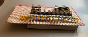
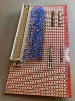
So...I have an update on this Flasher utility saga. I spent all day putting this together. I think this may be the jankiest LC PDS card ever created.
pdscard1.jpg
pdscard2.jpg

It brings out all 96 pins to a 3x32 header so I can attach jumpers. I don't need the extra 18 pins that newer models have. My PDS card also has a socket for a GAL22V10, headers for running jumpers to it, and a few small headers meant for 5V and GND. If you ever plan on doing this...just design a PCB. Don't do what I did. This took hours and hours to solder. It wasn't fun. But I had no choice...my free time is now, and a PCB would take too long to arrive.

I populated it with the bare minimum needed to make the CPU happy and programmed an ATF22V10C with my final design for acknowledging reads and writes sent to the PDS socket. Basically listening to a few address lines, R/W and /AS, and controlling /DSACK0 and /DSACK1 as necessary.
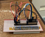
baremin.jpg

This worked. With nothing installed, reads to the PDS memory area result in a bus error:
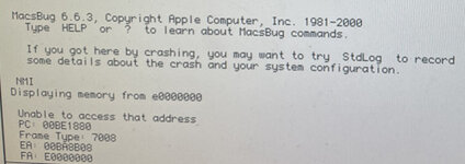
nocard.jpg

With my card installed, I read junk data of all 0xFF instead, meaning my PLD is doing its job!
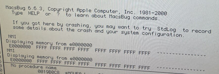
cardgood.jpg

So...you think my card looks crazy? You ain't seen nothing yet. Here's crazy:
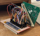
simmsocket.jpg

This is one of my bare programmer PCBs with jumper wires soldered and connected everywhere on my PDS card so bring out all the correct pins exactly where they go. All of the address and data lines of the SIMM socket go directly to the PDS connector. /OE and /WE go to the PLD -- it controls them with the right pattern when there's a matching read or write cycle. I also brought 12V to the SIMM socket for VPP for the Lobos board replica. Luckily, I already had this bare socket-to-jumper-wires adapter board from when I was working on the next-generation SIMM programmer. It was still a huge pain and took hours to get all of the wires hooked up!

Finally, it was time to insert one of my replica Lobos SIMMs and plug it into my LC 475 to see what happens. First, I made sure 12V wasn't accidentally shorted anywhere else on the board. That would be bad.
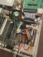
installed.jpg

Yeah...janky is definitely the right word to describe this setup! The corner of the bare programmer PCB is balancing on the CPU. Everything booted, which was a good sign. It meant I wasn't screwing up the address and data lines. Then I opened up Flasher, and...
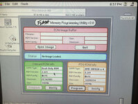
flasher.jpg

It works! The right side of the Flasher UI is populated with SIMM info. I can dump, program, and verify through it! This SIMM had a different image on it (I think it's my hacked 630 ROM with the 6200 chime). I was able to dump the 475's onboard ROM and program it to the SIMM through the PDS card, and everything worked perfectly!

I already got some hints about the purpose of the PDS card on my blog, so I'm kind of repeating what I already knew at this point, but these tests definitely confirm that the PDS card was meant for programming SIMMs (you wouldn't be booted from the PDS card). When you program a ROM image through this PDS card, the UI updates as you do it. It tells you that it's erasing, then programming, then verifying. Onboard SIMM programming didn't allow this, because you can't do toolbox calls while you're in the middle of programming the ROM you're booted from. Also, it just leaves you back in the UI when it's done -- no reboot like when you program the SIMM you're booted from. The status says "Successful" afterward.

So...I had to learn all about 680x0 bus cycles, how to program PLDs in WinCupl, tediously solder a whole bunch of wires, then tediously hook up a bunch of jumper wires that were way too short. But it was totally worth it! I have now proven the concept of a PDS SIMM programmer card. I think it may be worth it to design something a bit cleaner that's an actual PCB. If it could be small enough to fit in the 575, 580, and 630 it should work in them too.

This same approach should work for other 040 PDS slots too. The 610 might be the easiest since it has the funky card edge connector slot which I think would be super simple to make a board to plug into. The others would need the full 040 PDS connector which I know is harder to find. I think the PLD would have to be slightly more complicated too -- the LC PDS slot's read/write cycles are slow enough that I didn't have to do anything special with wait states to access 120 ns flash chips, but I'm pretty sure the direct 040 PDS would be too fast so I'd have to slow it down a bit. Nothing too crazy though...I think...

This is pretty exciting! It's the equivalent of my USB SIMM programmer, but Apple made software for using it and it's a PDS card instead!
 

tt

Well-known member
This is pretty exciting! It's the equivalent of my USB SIMM programmer, but Apple made software for using it and it's a PDS card instead!
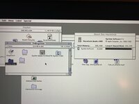
Insane work on the PDS card. That is an exciting proposition to have a retro machine being able to serve as a ROM programmer. Would it also work with an 030 LC III? I am not super familiar with the LC series PDS variations.
 

dougg3

Well-known member
Insane work on the PDS card. That is an exciting proposition to have a retro machine being able to serve as a ROM programmer. Would it also work with an 030 LC III? I am not super familiar with the LC series PDS variations.

Thank you tt! It was a lot of work. It was super duper satisfying to see it all work properly when I finished it.

That's a good question! Physically it should be compatible with the LC III since it's the same LC PDS slot. The 96 pin version of the slot goes really far back for compatibility, all the way back to the original LC. Newer, faster machines are still compatible with slower cards because they basically pretend to be the speed of an LC on that slot. Then around the time of the LC III they added more pins for some missing address lines and also adding the capability to use the slot in a non-slowed-down-for-LC-compatibility way. But they added it in a way that old 96-pin cards can still plug in.

The Flasher software doesn't seem to have any LC III PDS card compatibility, but I think it would be possible to add support. I think it would just be a simple matter of adding a couple of new table entries that look for this card with the LC III's gestalt ID, and set up the cache control registers properly.

Interestingly, the LC III is supported by another table entry, but it's for an onboard ROM SIMM. The final LC III board doesn't actually have provisions for a SIMM socket though. I'm guessing development versions of it did.

P.S. I haven't forgotten about getting replica Lobos boards to you and @Jockelill. It will happen eventually!
 
Top