• Hello MLAers! We've re-enabled auto-approval for accounts. If you are still waiting on account approval, please check this thread for more information.

Another IIci ROM hack

Ah, yeah...some kind of buffering would probably be needed. I forgot that it's not just a byte-per-byte write and erase thing when you're dealing with flash.

What about using an SD card rather than an SPI flash? I *think* an SD card would be easier because it will handle the wear-leveling internally and just present itself as a block device that can be read/written in 512-byte chunks. I don't know if that's useful at all, but I'm guessing the convenience of being able to pull the card out and plug it into the computer to be reflashed would be useful.

I know that write performance isn't the best with SD cards, but it's just a thought...

 
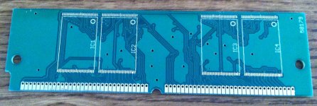
Yes the TSOP48 sockets i have sit right on the footprint the chip would go, its designed that way on purpose so you can pull the TSOP off a board, and put a socket in place so you can debug without in-circuit flashing ability.

I picked a few of these up and never used them.

Also, as far as the FPGA goes, does the RESET signal come to the ROM slot? i cant remember. if so, you can hold the bus into RESET until its finished loading. then free the bus. Dennis' method would work just as fine as well. But requires additional logic blocks in the FPGA to keep the bus in a loop. then once its complete, use a mux or something in VHDL to switch over. Nice thing about having this type of a setup, you can hot-flash the SPI inside the mac while its running with an application, as long as you have FPGA blocks to support it, without touching the RAM contents so the "ROM" dont change on the mac while your flashing it. Then reboot once done, if the RESET signal comes to the SIMM the FPGA can pick up this signal and start its entire SPI to RAM loading process over again. Regardless, i think you need to watch the RESET condition as a signal to start the process.

Either watch this pin, or decode the reset vector on the bus, if the FPGA detects it, reload SPI to RAM and hang RESET until complete. Since we are doing some real simple tasks, i think a micro FPGA would work just fine, and would fit on the SIMM. The only drawback is finding an FPGA that runs on 5V only. most are 3.3v, 1.8v, or a combination of voltages. one for IO, one for Core, etc... in which case youll need small SOT-89 V-Regs on the board to handle this, some 3.3V FPGAs are 5V tolerant so make sure you look at that aspect as well, it could be a trap if no attention is paid. ;-)

there are some open-source softcores too so if you wanted to put some "brain" on the SIMM for advanced operations outside of logic, in theory, you could such as the flashing algo for SPI would have to be run on a softcore unless you know of a way to code it specifically as logic in VHDL. If you ran out of on-chip storage, you could always compress the code that would run on the softcore and expand it at the "end" block of the RAM chip and boot the code from there for the softcore to SPI flash, etc... many many many options.

Hell if the architecture supports cache RAM, you could add an FPGA block to address out some RAM space for caching. speed up the machine.

Sorry for the rambling, its just some info. I am FPGA dumb, but i do know how they work to an extent, and learning as I go.

 
This gets me thinking about microcontroller vs. FPGA because talking in serial is good for microcontrollers and talking right away in parallel is good for FPGAs. I'm starting to wonder if we could get by with just a microcontroller. FPGAs are fairly complicated to program in my experience.

I haven't seen it done much in the hobby world, but maybe USB could be an option? I've heard that hosting USB has a lot of overhead. USB opens the door to flash drives, hard drives, and USB-to-memory card converters. I'm thinking that you get non-SPI, high-speed access to SD cards that way. Using a microcontroller also adds the possibility of filesystem support, so you can store the ROM data in a file on the USB storage device, allowing you to mount the USB device on a computer and copy / modify the file. A ROM burner or special application would no longer be necessary.

 
Last edited by a moderator:
the thing is, the microcontroller would have to be very very fast, as you would need a bit of headroom between bus cycles. and then you need DRAM controller/timing code for DDR chips or whatever RAM you use. Thats why i think an FPGA would be better suited but use a softcore for the MCU part of the tasks.

an MCU alone is sufficient if your loading from a storage medium or etc to Shadow RAM for the ROM. But the bus handling of the RAM is where things get tricky. You need headroom between each bus cycle so you can do things such as refresh the RAM, fetch the data, etc.. So when the bus cycle comes the data is ready for it, and it has to be fast between each phase. So when the address phase comes, the CPU can quickly refresh and fetch the data from the RAM to be put onto the bus. It could be doable, but your not doing it with your standard 8-bit micro. you would almost need a propeller which has multi-cores, or maybe an ARM based MCU with fast I/O.

You basically would have to calculate the time period that would occur between each complete bus cycle at its fastest possible point it ever could, and each phase within the bus cycle, that way you can pick up a suitable microcontroller and speed that would be able to get quite a few machine cycles completed within that period. Then youll be ok.

So if for example the MCU can execute at least 10 to 12 instructions between a cycle period, maybe 4 instructions between a phase period then if you keep things fast and tight, its doable to fetch the data in time.

 
I'm not totally straight on how RAM sticks work on a signal level. I understand that something has to go through and refresh the contents of RAM constantly. Is this process within the realm of a microcontroller's ability? Also, for this RAMmish ROM SIMM, can address and data connections be made directly to the RAM so that the Mac talks only to the RAM and not "through" the microcontroller / FPGA? Or does there have to be logic between the RAM stick and Mac's busses?

If the Mac can interface directly with the RAM, and if the ROM data is in the RAM, then it should be able to read it right away regardless of how slow the microcontroller is?

 
I dont know the full detail on how RAS/CAS timing and refresh cycles work, but i do know that on an ATmel AVR series microcontroller, it barely has enough speed to run and refresh 30pin SIMM type DRAM. its been done, but its not a good candidate.

There is open source VHDL code out there for DDR1 2, and 3 RAM chips for reading/writing/controlling those ICs maybe looking at that could turn up some results on how they work? I guess the RAS/CAS/CL numbers you see on computer RAM sticks is the requirements to keep the data inside valid...

But as far as being able to bus directly to the RAM, i dont know. I dont think so because the FPGA or DRAM controller has to mux itself in at some point to refresh the RAM. If you look at the SE/30 schematics there is a PAL chip and several muxes that do just this.

the memory/system bus via the PALs are timed in such a way that when a read or write operation happens to the SE/30 RAM, it always occurs in between the refresh cycle, it does not occur right at the same time the RAM is being refreshed, so the bus doesnt get halted or some type of GPF occurs. I have studied that circuit until my eyes went crosseyed for troubleshooting reasons, and thats what I have gathered.

 
Here is another more detailed, and newer document that goes into SDRAM and DDR:

http://smithsonianchips.si.edu/ice/cd/MEMORY97/SEC07.PDF

with SDRAM you can do concurrent operations, such as refresh AND read at the same time, So no collisions.

But you still need some logic. Why? because DRAM is broken into rows and columns so you would need an address decoder at the minimum to turn an address into a row/column fetch, in sync with a counter that keeps refresh as well. This way the fetch is valid and the RAM is still being refreshed. The returned data can be placed onto the bus when the bus requests the OE. This is simple mux/counter/decoder logic in a FPGA, or code in an MCU, with MCUs though you have to keep an accurate sync on the bus or you can get race/lag conditions. lol. I am not sure of the window on ROM as in how fast the data needs to be on the bus at the time of an address/fetch. RAM is like 70 to 140ns, ROM i dont know. but you have to be within that window or it may not boot so if the MCU takes too long to fetch the data out of RAM with a given address, your up shit creek without a paddle.

 
Basically in a nutshell, your using the FPGA to do one main purpose. To convert the DDR Dram into PSRAM. which basically looks like regular SRAM on the bus. as SRAM and ROM are accessed identically, only difference being SRAM is temporary and ROM is well, permenent aside bitrot.

You actually might be able to buy PSRAM outright with the refresh controller actually built into the IC. If thats the case, you can use it as SRAM and dont need any FPGA or associated circuitry. Just an MCU to copy SPI flash or other source to the RAM before boot.

P.S. Matter of fact, here is a document to do just that...

http://www.fujitsu.com/downloads/MICRO/fma/pdf/psram.pdf

life just got ALOT more simple. You will still need at least minimally an MCU and mux to switch it off the bus during a write. Also PSRAM is still in active development because its used for low-power/mobile market. Also do you want to upgrade the memory in your mac portable? yea.. welll.... thats a possibility too.

128Megabit (8Megabyte) PSRAM chips are cheap too, between 6 to 11 dollars depending on who you go with. They are BGA mount however, but they are MBGA48s which are simple to mount with a heatgun and a hotplate/pancake griddle. I used to mount EBGA64s this way.

Datasheet:

http://download.micron.com/pdf/datasheets/psram/128mb_burst_cr1_5_p26z.pdf

That chip is perfect. 16bit I/0, 22bit addressing. 128Megabit chip, which is 8megabytes or 4megawords. being that its a 16bit output, you would see 2 bytes at a time. These chips are also about $13 from digikey. probably cheaper than 4 flash TSOPs, but you still have to factor in the logic for the processor required to put the information INTO the RAM ;-)

 
p. 33 8-o

This discussion got too far above my head for a bit, so I've ignored it for a while. Looka like I'd better get current on this while I have a chance!

Meanwhile, back to simple problems. DQ & Company, when you test all these different ROM/Mac combos, the Gestalt IDs remain the same when a new combo works, correct? Could the Gestalt Id's five bits of information be simple component(s) on the MoBo that are addressed over I2C before the CPU queries the ROM addresses?

I need to tell my IIsi that it's something like a Quadra 700. That way the Radius Rocket,RocketWare Installer a/o RocketWare itself, will think it's compatible with the Stealth IIsi.

Whatcha think guys?

 
The gestaltMachineType values are based on what the ROM detects from the hardware. AFAIK, this value is an ultra-boiled down version of what the GetHardwareInfo/GetExtHardwareInfo ROM routines generate. Those routines are somewhat complicated (I just went over their disassembly yesterday) since there's all kinds of different ways various boards identify themselves, but for the machines covered by the Guide to the Macintosh Family Hardware, it is mostly determined by VIA values as documented in Chapter 4.

For other machines, the MESS guys have some information in their Technical Notes

But, as has been covered before there are many ways to try to check what machine you're on. "Wish I Were" changes the gestalt value (which is easy to do, like I did for the system version gestalt, so I doubt they're looking at just the gestalt value.

All that aside, the first thing you need to do is determine what they're checking. My suspicion is, in the end it'd just be better to patch RocketWare.

 
AFAIK, this value is an ultra-boiled down version of what the GetHardwareInfo/GetExtHardwareInfo ROM routines generate. Those routines are somewhat complicated (I just went over their disassembly yesterday) since there's all kinds of different ways various boards identify themselves, but for the machines covered by the Guide to the Macintosh Family Hardware, it is mostly determined by VIA values as documented in Chapter 4.
I'm wondering, if the DayStar 601 gets the gestalt from the ROM routine, if it were patched to return the IIx code, then maybe it would enable compatibility for an SE/30. }:)

 
Oh. I just sold my 601, otherwise I'd 've let you guys borrow it and play around. I got rid of it because 99% of my software is 68k, and the 601 card was actually significantly slower than my 040 card. I have DP 1GHz QuickSilver if I need PowerPC. :p Plus, my custom ROM is designed to work with my 040 card and I really, really like my Arrr! startup sound and Pirate Mac icon.

 
Yes, definitely not practical... more of a proof of concept. I still have mine. It gets as far as sounding a powermac boot chime. I'm thinking it gets tripped up on the video/NuBus or gestalt code.

 
OK...I got a SIMM all assembled:

Assembled.JPG

I was able to put my 2 MB huge mario startup chime ROM onto it and it worked fine booting the IIci--so I definitely wired the circuit up correctly and got the unlock sequence correct. Then I washed the board and now it's having some trouble with corrupt data on one of the chips when I flash a full 8 MB file to it. I think I just have to play around with it a bit and it will be fine. I might have a loose solder joint or something like that. It's passing my electrical test so I don't think it's a shorted pin. Once I figure out what's going on, I think it will work...the other three chips seem to flash fine through the entire 8 MB of space. And it definitely worked earlier before I washed the board.

It takes almost 8 minutes to flash the entire SIMM...so it's not very much fun waiting for it to complete when I want to test things :)

I have already ruined a PCB (lifted a pad) and one of the flash chips (broke off 2 legs) carelessly playing with different soldering techniques--I accidentally bent one of the legs and tried to un-bend it with my soldering iron...bad idea...

Looks like a small iron tip is also a bad idea...a normal size iron tip, plenty of flux, and copper braid is definitely the way to go with this fine pitch stuff. I wish I could get good enough to where I don't need the copper braid at all, but it's really tough not to create shorts on pins so close together. Despite the tiny size, I think once I have more experience soldering fine pitch components, this SIMM will be easier to put together than the 2 MB SIMM.

Edit: I found a few places where there were some questionable-looking solder joints on the chip that was causing problems, and it works now! My IIci is playing the first movement of Beethoven's Moonlight Sonata to me right now...the 8 MB SIMM can fit an entire almost-6-minute performance of it as a startup chime. Perfect way to test the SIMM out -- it's working! It's ALIVE! I can now confirm that the IIci has all of its ROM SIMM address pins wired up correctly. This is going to work! :)

 
Back
Top