demik
Well-known member
Hello,
Noticed a few month ago that the 53C80 SCSI Chip is in life production by Zilog, available new :
Mouser link : https://www.mouser.fr/ProductDetail/692-Z53C8003VSG/
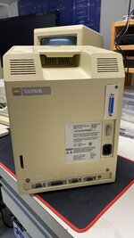
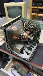
COVID helping, I bough a broken MacSnap SCSI on eBay and started to reverse it. I though it will be cool to gave a schematic and understand a little bit how it was done.
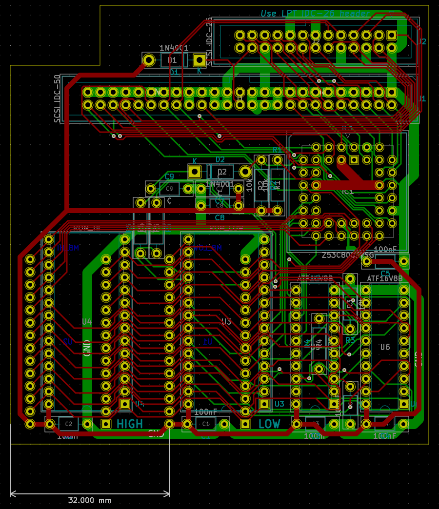
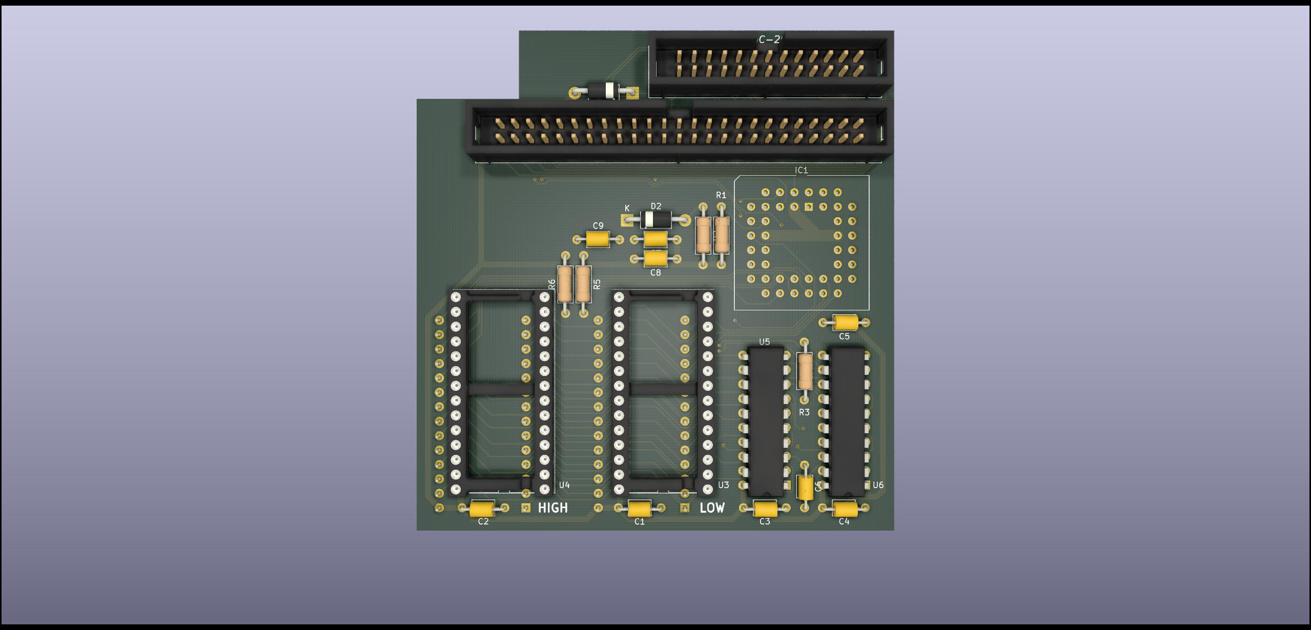
Managed to buzz almost everything and new PCB is almost done (and converted for use with a PLCC SCSI chip).
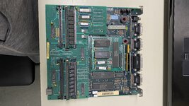
The board consist of :
- 53C80 SCSI chip
- Custom timer circuit to reset the 53C80
- two PALs
You can find a good article written by @Dog Cow on his blog here :
https://macgui.com/news/article.php?t=471
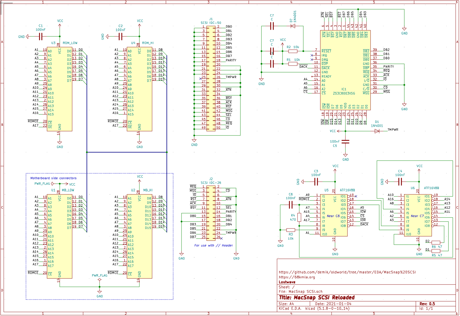
Here is the reversed schematic :
Currently I've got a few issues :
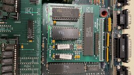
Resistor Packs
The original board got three resistors packs (~ 150Ω each) wired to each output of the 53C80 chip to the ground. I double checked with the MacPlus diagrams and the Mac Classic Ones, and neither of them have those resistors ladders. Any ideas what they are for ?
PAL
What is going on with the two PALs ?
The left PAL looks to be used as an address decoder to generate /IOR /IOW /DACK and /CS lines and a few other stuff.
The right one is especially weird. I cannot understand why it's wired that way... It has freaking data lines ! This is straight dark voodoo stuff. Only possibility I came to is that it's used to "live" patch the Mac ROM while running. Is that even possible ?
You can read on the PCB "128k ROM ONLY", so that could be it... 128k ROM as "Mac 128k" or 128k sized ROM (MacPlus) ?
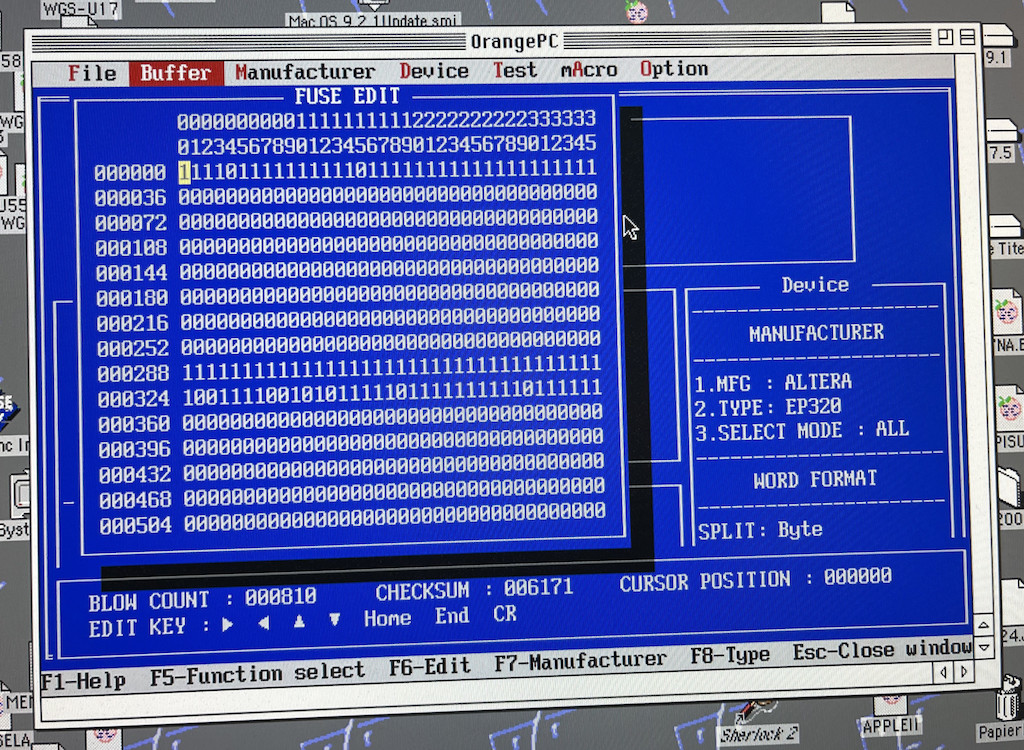
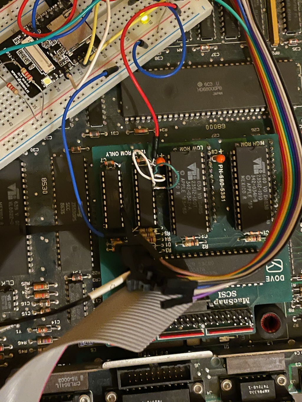
Here is a picture of the board :

I will get a PAL Dumper soon, but my hopes aren't high...
Would creating a new custom PAL be a better idea ? I think creating only /IOR /IOW /DACK and /CS lines should be enough. But we have a limited number of address lines though the ROM socket so that will be tricky.
- /ROMCE should be good for 0x40 0000 to 0x5F FFFF which include SCSI space (0x58 0000 to 0x5F FFFF)
- /CS should need A19:A23 but we only got access to A1:A17
- /DACK don't understand very well what's its for. Looking at the Datasheet, it's used for DMA purposes, but from what I remember, neither the Mac 512k / Plus / SE support DMA.
- A9 + /ROMCE can be used to generate ~IOR and ~IOS, but what about the other ones ?
Let's say ROM data is between 0x40000 and 0x42000, so generate /CS between 0x58 0000 to 0x5F FFFF when /ROMCE is low ?
Other informations
Does anyone have a manual for this board ?
Thanks for your help or input.
Noticed a few month ago that the 53C80 SCSI Chip is in life production by Zilog, available new :
Mouser link : https://www.mouser.fr/ProductDetail/692-Z53C8003VSG/
COVID helping, I bough a broken MacSnap SCSI on eBay and started to reverse it. I though it will be cool to gave a schematic and understand a little bit how it was done.
Managed to buzz almost everything and new PCB is almost done (and converted for use with a PLCC SCSI chip).
The board consist of :
- 53C80 SCSI chip
- Custom timer circuit to reset the 53C80
- two PALs
You can find a good article written by @Dog Cow on his blog here :
https://macgui.com/news/article.php?t=471
Here is the reversed schematic :

Currently I've got a few issues :
Resistor Packs
The original board got three resistors packs (~ 150Ω each) wired to each output of the 53C80 chip to the ground. I double checked with the MacPlus diagrams and the Mac Classic Ones, and neither of them have those resistors ladders. Any ideas what they are for ?
PAL
What is going on with the two PALs ?
The left PAL looks to be used as an address decoder to generate /IOR /IOW /DACK and /CS lines and a few other stuff.
The right one is especially weird. I cannot understand why it's wired that way... It has freaking data lines ! This is straight dark voodoo stuff. Only possibility I came to is that it's used to "live" patch the Mac ROM while running. Is that even possible ?
You can read on the PCB "128k ROM ONLY", so that could be it... 128k ROM as "Mac 128k" or 128k sized ROM (MacPlus) ?
Here is a picture of the board :
I will get a PAL Dumper soon, but my hopes aren't high...
Would creating a new custom PAL be a better idea ? I think creating only /IOR /IOW /DACK and /CS lines should be enough. But we have a limited number of address lines though the ROM socket so that will be tricky.
- /ROMCE should be good for 0x40 0000 to 0x5F FFFF which include SCSI space (0x58 0000 to 0x5F FFFF)
- /CS should need A19:A23 but we only got access to A1:A17
- /DACK don't understand very well what's its for. Looking at the Datasheet, it's used for DMA purposes, but from what I remember, neither the Mac 512k / Plus / SE support DMA.
- A9 + /ROMCE can be used to generate ~IOR and ~IOS, but what about the other ones ?
Let's say ROM data is between 0x40000 and 0x42000, so generate /CS between 0x58 0000 to 0x5F FFFF when /ROMCE is low ?
Other informations
Does anyone have a manual for this board ?
Thanks for your help or input.
Last edited by a moderator:


")