• Updated 2023-07-12: Hello, Guest! Welcome back, and be sure to check out this follow-up post about our outage a week or so ago.

Reverse Engineering the Macintosh SE PCB & Custom Chips for 1:1 reproduction

Kai Robinson

Well-known member
It may be possible to bypass the code protection using glitching techniques for fault injection. But unless there's a documented method for this series of chips or someone experienced with glitching, it might just be easier to re-implement. I have code for at least one Apple ADB controller, but it's a much later version.

I find it surprising that your first step wasn't to create schematics. Doing layout directly just sounds like too much effort to me. But you get to do your project your way! [:D]
 Yeah, i'd looked into it, but it's beyond me, the glitch stuff - especially on MCU's this old - i'd be scared of barbecuing it!

As for the schematic - oddly, tracing back the schematic is easier using the sprint layout, because you have the 'test pin' function - which shows all tracks connected to a pin, what goes to where etc. 


techknight

Well-known member
Now we are 20 pages into this thing, Whatever happened to the 1:1 clone? 

Did it ever work after the 3rd run of the PCB? or? 


techknight

Well-known member
@techknight Waiting on a 'scope so i can see what's going on with the clock line and if the CPU is held in reset, if there's any activity from the ROM's


Oh I must have missed a part somewhere. So it didnt work? 

Last thing I saw is you had a bad power supply or something. 

sorry, its hard for me to follow since there is a few different conversations going on in here. 

 
Last edited by a moderator:

Kai Robinson

Well-known member
@techknight Well, more more out of it than before - the A5 line was patched to the ROM's, and fixed in the Sprint layout as well - but i'm concerned that the ROM/BBU/Oscillator might be at fault here. Yes, the voltages are shonky from the power supply, but a recap will sort that.


techknight

Well-known member
@techknight Well, more more out of it than before - the A5 line was patched to the ROM's, and fixed in the Sprint layout as well - but i'm concerned that the ROM/BBU/Oscillator might be at fault here. Yes, the voltages are shonky from the power supply, but a recap will sort that.


Wheeeee well lets hope its an unconnected trace or something somewhere. 


Kai Robinson

Well-known member
I've scoured the board - i can't find anything else anywhere that could be the issue - the only thing i can think of is the customs or the clock is wonky. The contents of RAM are being displayed at least - so the video circuitry is good, there's obviously SOMETHING in RAM...i built that 27C010 ROM adapter specifically to use a clean image on new ROM's that aren't bent legged, tarnished or potentially a bit on the duff side. 


quorten

Well-known member
@asicsolutions  Main point in hand, the reverse engineering efforts on the Macintosh SE are a good stepping stone to a reverse-engineered SE/30.  The GLUE is the SE/30's more sophisticated version of the BBU in the SE.  Our collective memory has forgotten many times... but I squinted really hard at that one grainy schematic so now we have a clean vector graphics version that is fairly accurate.  It's an SVG.  (With transparency, so you want to open it in a window of its own.)

retrace_se_mlb_p1.svg


https://github.com/quorten/macsehw

Together with the SE/30 redrawn schematic, I have felt this was plenty of pristine info for designing the BBU replacement.

A quick update on my progress in the BBU, right now I'm focusing on fixing up a few hiccups in the overall design idea before writing the simulation test bench.  Mentioning RAM SIMMs, I'm still not sure how the 4MB DRAM refresh works but the framebuffer scanning circuitry definitely does double as refreshing the DRAM if there is <=1MB of RAM installed.  It would be great if other folks could read into the lines and come up with an explanation for this.

I will admit I got a bit sidetracked from BBU implementation efforts by a DIY GPGPU design project of mine... but point in hand, having a simplified MC68000-like RISC CPU is what I plan on doing for the simulation test bench of my BBU re-implementation design.  Just to do things like respond to interrupts, fetching boot code from ROM, execute RAM test, etc.

 
Last edited by a moderator:

Kai Robinson

Well-known member
@quortenreal life gets in the way for me a lot lately - work is being a particular pain in my arse, hence the slow pace on the project lately. Will try and ramp up in the new year a bit more as well. 

One thing i thought of - Pins 19 and 24 of the 30-pin SIMM slot aren't connected at all, because the BBU doesn't have enough pins to break those out as well as everything else hence the 1MB SIMM limit and 4MB overall limit (2^10bit x 1 = 1024KB and 2^12bit x 1 = 4096KB).

To be fair, in 1987, the concept of 4MB of RAM was utterly beyond what most people would have ever been able to use on that platform, so I can see why that was done. For a BBU replacement that fits the pinout - it'd be possible for me to break out those two pins for both banks easily enough, to a header nearby (route through the ground plane to be sneaky like snek), so you could control the additional two address lines - voila - 16MB capable Mac SE - assuming nothing needs to be changed with the ROM's.

@techknight i had the thought of making a piggyback board for the CPU socket, to replace the original ROM's entirely...to allow the use of the ROM from the Mac Classic - not sure what advantage it'd be over the LOW/HIGH ROM arrangement, other than ROM bootable System 6 :)

Mad ideas or is this the beer talking? :D

 
Last edited by a moderator:

Phipli

Well-known member
I think I remember that the RAM refresh is linked to the screen drawing and so you need to do more than break out the address lines - the design was optimised by linking the two, but it means there isn't RAM refresh circuitry for much more than 4MB... I'm likely to be mis-remembering :/


quorten

Well-known member
@Phipli That is correct in abstract, but do you have more details?  I can see that the Macintosh Plus relies on software to refresh the high portion memory (RA9 on the row access strobe) of each 1MB DRAM SIMM, but I have no idea what this is exactly.  For the Macintosh SE, it would have to be a software routine that continuously scans a contiguous 2KB buffer (or larger) anywhere in the first 512KB of RAM.  The low memory (RA0 - RA8) is refreshed entirely by the readout of the framebuffer scanning circuitry.


Phipli

Well-known member
@quorten I'm trying to work out where I read details, or if I ever did. There is some info in the "Guide to the Macintosh Family Hardware" but I've not found a full description - the other place I might have seen it is in "Designing Cards and Drivers for the Macintosh II and SE", but I haven't checked yet. I'll keep looking. Are there any memory map issues? I know expansion boards tended to implement extra RAM using virtual memory and a RAM disk. I'm several steps beyond my understanding though as I've only ever read stuff to do with SE RAM with a passing interest, rather than with the intention to understand its functionality in detail.


quorten

Well-known member
I revisited the Macintosh 128k PAL equations I have and touched them up to something more functional... and well, although it's still not quite accurate to the original Macintosh PALs, I feel I've learned quite a bit about the canonical way to implement replacement logic as close to the original as possible.  In hindsight, it probably would have been a good idea to consider doing a more rigorous study of the older Macintosh hardware before diving into the SE.  However, the Macintosh SE logic board is arguably easier to replicate due to its integration of all custom logic into a lesser chip count.

 
Last edited by a moderator:

techknight

Well-known member
@techknight i had the thought of making a piggyback board for the CPU socket, to replace the original ROM's entirely...to allow the use of the ROM from the Mac Classic - not sure what advantage it'd be over the LOW/HIGH ROM arrangement, other than ROM bootable System 6 :)

Mad ideas or is this the beer talking? :D


only reason the Low/High ROM exists is most ROMs back then were 8-bit data bus. so they needed both ROMs to achieve 16-bit bus transfers. 

Now, the question is, if the Classic's ROM chip has the ability to perform 8-bit transfers as well as 16-bit transfers, using Upper/Lower strobes, as this is important to the operation of a 68K. So, youll need that. 

The other question is, are the Classic's ROM drivers compatible with the SE? are the hardware registers and peripherals, etc mapped in the same memory locations? 

 
Last edited by a moderator:

Kai Robinson

Well-known member
Well, i was a very lucky boy for Christmas and santa brought me a new DS1102 Oscilloscope! Along with a Yihua 959D Hot Air station - I've just bought a Meanwell RT65B which has all the right voltages with enough current to set this up as a bench PSU for the board. I can monitor the video out signal on the scope. I tried in a separate SE/30 chassis but still no dice. I'm not getting anything. I think @techknight is right - there's a clock signal missing or not quite right somewhere. 


techknight

Well-known member
Well, i was a very lucky boy for Christmas and santa brought me a new DS1102 Oscilloscope! Along with a Yihua 959D Hot Air station - I've just bought a Meanwell RT65B which has all the right voltages with enough current to set this up as a bench PSU for the board. I can monitor the video out signal on the scope. I tried in a separate SE/30 chassis but still no dice. I'm not getting anything. I think @techknight is right - there's a clock signal missing or not quite right somewhere. 


Yea, something is going on. id probe the Strobes, 8Mhz clock, etc. and see if the CPU is even doing anything. 

And.. Nice on the equipment :)

I have a fluke scopemeter, thats about it. 

 
Last edited by a moderator:

Kai Robinson

Well-known member
only reason the Low/High ROM exists is most ROMs back then were 8-bit data bus. so they needed both ROMs to achieve 16-bit bus transfers. 

Now, the question is, if the Classic's ROM chip has the ability to perform 8-bit transfers as well as 16-bit transfers, using Upper/Lower strobes, as this is important to the operation of a 68K. So, youll need that. 

The other question is, are the Classic's ROM drivers compatible with the SE? are the hardware registers and peripherals, etc mapped in the same memory locations? 


Yep - the TC534200 is selectable 8/16-bit access, either as 256k x 16bit or 512k x 8bit. I would imagine that there's 0 difference between the classic and the SE, all the hardware is identical, just that the classic uses SMT to reduce board size and cost - they share the same BBU and peripheral support chips. 

View attachment TC534200 Datasheet (Classic ROM).pdf

 
Last edited by a moderator:

Kai Robinson

Well-known member
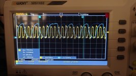
Ta-da! New scope, new data! 

Main Oscillator is outputting correctly and the 3.7MHz from the BBU/Glu is working fine, too. 

There is a 7.83MHz clock on the 68000's CLK pin, but there is no activity on the address or data bus, except random noise from the SIMM end of things. 

DSC_0396.JPG


Kai Robinson

Well-known member
Replaced the 68000L8 with a 68010P10 and still no dice. I'm not convinced that one is working either - so i've ordered a few 68000's to be sure. Still nothing on either the address or data bus. 

 
Top