Very cool! How difficult was it to build and is there any special equipment needed?
TLDR: Difficult, expensive and with some major caveats!
The longer story:
The carrier card itself, is very straightforward, solder on headers, solder on 040 connector, install FPGA-card, done. BUT, and a big such, programming the FPGA is a little bit difficult (you need to use either an Intel Mac with terminal or a Linux machine, and general knowledge of terminal commands, java compilation, firmware flashing etc). Reason why it will not work on an ARM - Mac is because the USB4JAVA library used by ZTEX is not supported on ARM-MacOS! Took me some time to fiugre out just that
")
. Getting the 040 PDS connector is somewhat of a challenge, I've only found them at one place with an MOQ of 1,
https://www.questcomp.com/part/4/p50-140s-rr1-tg/301253758 but they are 16$/pcs.
The 040 connector has a fairly tight pitch of 1.27mm and three overlapping rows (160pins in total), so it's quite a lot to solder and you need a thin tip.
The major drawback is also the overall cost, just the FPGA is about 250$, connector about 16€ and carrier card about 60-70$ depending on where you get it, so you're looking at something like 350-400$ just to build it (with freight costs and stuff). The FPGA can be reused for all versions, but must be reflashed for every carrier card since the FPGA bitstream differs.
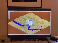
Another drawback would be that only 1920x1080 is supported as a "true resolution", for every other resolution it will be windowed with an increasingly larger black box around it. I'd say down to 1280x1024 is still very much useful, but the classic 640x480 will be very small even on a 27"-32" screen and not very playable for old games. I know
@Melkhior has looked very exensively at this, and there might be a fix for it in the future (FPGA Experts where are you??!). On the bright side there are surprisingly many games and programs that actually do support the full resolution. Both Simcity 2000 and Civilisation II will be full screen!! And also Excel, Word, Photoshop etc
I'd say for now it's very much in a beta phase, but to the point where it still offers a lot of usefulness!! I'm running my Q650 and IIci with FPGAs since quite some time here, I started with the NubusFPGA in my IIci (also from
@Melkhior) and now switched to the QuadraFPGA for my Q650. I also have the IIsiFPGA which I will explore some time after the holidays.
Another issue is that the "low-cost" 2.13a model is no longer available. Ztex replaced it with a 2.12 version, but
@Melkhior had some serious issues with it, so it's a big no go for now (we are wiating for feedback from Ztex). The carrier will work with all other models of the 2.13, so you can also use the 2.13b, but the price is higher at 229€:
If you still want to build one, feel free to reach out to me on a PM, and I can share all my experience. JLC has an MOQ of 5 boards (whereof 2 must be mounted), but there might be others interested to share the cost.
Compatible machines should be all machines with 040 PDS, so Q650, Q700, Q800, Q900 and Q950. The Q840AV does not have a PDS, so here you can only use the slower NubusFPGA. Q800/650 are very good candidates, or the Q950 since all of them can be safely overclocked to 40Mhz and beyond (
@eharmon can tell you all about overclocking
)
@Melkhior has done some other really cool stuff like overmapping the onboard DDR3 memory from the FPGA with the machines RAM, so you can increase your Q650 all the way up to 776MB of RAM (with an hacked ROM to support 128MB Simm modules).
If you "just" want a new nice graphics card to get HDMI from your vintage Mac, I'd honestly recommend getting something like a scaler instead, safer, easier and works "out of the box" (well, sort of...), but IF you like to hack, tweak, tinker, self inflicted pain gets you going and you get high on the sensation of partial successes no "normal people" would ever grasp, well, then your're definitely in for a real journey!!