• Updated 2023-07-12: Hello, Guest! Welcome back, and be sure to check out this follow-up post about our outage a week or so ago.

Help understanding LC PDS 68020 bus cycles

dougg3

Well-known member
I've been tinkering with trying to recreate an LC PDS card that I'm pretty sure existed inside of Apple at some point: a ROM Flash SIMM programmer supported by Apple's Flasher app, at least for the Quadra 605 and LC 475. I wrote a blog post about it a while back where I described getting it working with a protoboard. Basically it's just a PDS connector, ROM SIMM socket, and a 22V10. It's a pretty simple concept. It forwards 32-bit read and write cycles to a flash SIMM, and Apple's Flasher app does the rest. I replicated the Lobos board from this thread and tested it with AMD and Intel 28F020 chips, both of which are supported by the app. I've been testing it in my LC 475.

Long story short, @Jockelill turned it into a PCB, much cleaner than my rat's nest. We've been doing some tinkering with it off and on. I've come to the realization that it doesn't quite work correctly though. Maybe it's not so simple after all. It wasn't working with the Intel 28F020 chips (verification errors early on during programming) until I accidentally realized that probing my generated /WE signal with my oscilloscope fixed the problem, which led me to try delaying its falling edge through a register. That also fixed the problem. However, I don't really understand why it fixed it because I didn't have any setup time issues with the address and /WE.

I've been really buckling down and studying the 68020 user manual's timing diagrams on pages 282 and 286, and the write cycle description starting on page 80. I was wondering if some of the amazing smart folks here would be willing to double check my understanding of what's going on. I'm having a hard time figuring out how I can meet all of the timings.
  • ATF22V10C-7:
    • Propagation delay: min = 3 ns, max = 7.5 ns
  • Intel N28F020-120:
    • /WE falling edge address min setup time: 0 ns
    • /WE falling edge address min hold time: 40 ns
    • /WE rising edge data min setup time: 40 ns
    • /WE rising edge data min hold time: 10 ns
    • /WE min pulse time = 60 ns
  • Am28F020-120:
    • /WE falling edge address min setup time: 0 ns
    • /WE falling edge address min hold time: 50 ns
    • /WE rising edge data min setup time: 50 ns
    • /WE rising edge data min hold time: 10 ns
    • /WE min pulse time = 50 ns
  • Am28F020 seems to need more setup/hold time, so I'm shooting for its specs for setup/hold, and Intel's for minimum /WE pulse width.
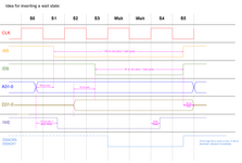
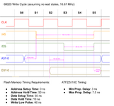
Here's a diagram I've come up with based on trying to follow the timing specs in the 68020 user manual. For LC PDS cards, Apple's documentation says I need to meet the timing requirements of the MC68020. The LC PDS clock is 15.6672 MHz. I'm going with the example timings that the manual lists for 16.67 MHz -- close enough. The timings of output transitions are not to scale. I put them in the middle of states because clearly based on the delays listed in the manual, they don't happen directly on the clock edges.

1722399712885.png
What I'm lost about here is, how do I meet these specs by only looking at CLK, /AS, and /DS?

My first naive approach was just to use AS to generate the /WE and /OE pulses. As long as my card is selected, /AS being asserted also means /WE or /OE is asserted (depending on RW). This actually worked okay on the AMD chips, but failed with the Intel chips. I did realize from the amazing knowledge in this post that I need to drive DSACK0/1 high afterward briefly because otherwise it goes back up noticeably slowly, so my first tweak to the logic used a register to drive it high for a clock cycle afterward. I did that and it looked much better on the scope, but it didn't fix the compatibility with the Intel chips.

Thinking about this simple approach in terms of setup and hold time:

The chips don't need any address setup time, but there is more than enough anyway (15 ns + 7.5 ns 22V10 propagation delay). Since /WE stays asserted the entire time /AS is asserted, it also has more than enough address hold time.

Data setup time is where it gets a little trickier. The /WE rising edge will be when /AS is deasserted, which gives it tons of setup time, but only 15 ns of hold time before the data becomes invalid. But when you take into account the 22V10's propagation delay (3 to 7.5 ns) before /WE goes high, the hold time is really somewhere in the ballpark of 7.5 to 12 ns. This doesn't necessarily meet the requirement for 10 ns of hold time.

Does my datasheet interpretation (and math) check out here? Based on this, I don't understand why delaying the /WE falling edge through a register actually fixed compatibility with Intel chips. It added more setup time that I didn't need anyway. Maybe the real problem is that I'm not meeting the data hold time requirement, and tinkering with other timings made it unexplainably start working? Maybe Apple's ASIC that pretends to be a 68020 bus for the expansion slot doesn't quite behave exactly the same as a real 68020? Can anyone think of any other explanation?

How can I move things around to obtain more data hold time after my /WE rising pulse? I assume it means I need to figure out how to make /WE go high earlier, but I don't know what I can use for that other than maybe looking at when /DS goes low. If I delay the /DS falling edge through a register and use it to generate the /WE rising edge, it seems like that would leave me with /WE falling somewhere in the middle of S1, and rising at the S3->S4 transition. Theoretically that would give me over 60 ns of /WE pulse width, but I'm not convinced that it leaves me with enough data setup time since the data only becomes valid sometime in the middle of S2.

Do I need to insert a wait state to give myself more time to work with? Am I misunderstanding something about how these bus cycles work? My head is spinning in circles and I'm crying uncle. If someone out there wouldn't mind checking my work or at least talking it out with me, I would greatly appreciate it! Thank you!
 

dougg3

Well-known member
I thought about it more and came up with this idea, basically delaying /AS through a few cascaded registers so that I can generate a delayed /DSACK to force a wait state, and also decide exactly when to do a /WE rising edge:

1722450396472.png

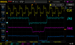
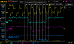
This seems like it meets all the timing requirements. But when I try this idea out on hardware, I get failures during programming. I even tried delaying the falling /WE edge to the next rising clock edge just to see if it would change anything -- it didn't. It looks like this on the scope (with the delayed falling /WE edge added):

1722450653541.png

As far as I can tell measuring things, I am now providing plenty of setup and hold time on /WE, plus the pulse is well over 60 ns. It's adding the wait state just as I asked for. Obviously I don't have /DS available to look at, but my rising /WE edge should be well past the point where /DS would have said the data is good.

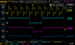
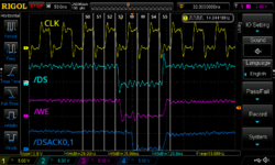
But it doesn't work! Not even with my scope probes attached. This simpler design with no wait states, that seems iffy on meeting the flash chip hold time requirements on the rising edge of /WE, works fine:

1722450860270.png

I'm so confused. I must be missing something. Why is it that a slower design with better timings doesn't work, but a faster design that I think violates the flash chip's hold time requirement does work? 🤯
 

zigzagjoe

Well-known member
Why not just use /DS as the trigger for your strobes? That is what I do personally on a few flash implementations I've done, and don't use /AS at all. Should have appropriate setups for both address and data by that point.

Concur that inserting a wait state would be ideal to extend the /WE pulse, you should be able to send /DS through a register and only generate your low-going /DSACK on that (but go high immediately on /DS going high). Might need two, can't recall fixed GAL polarities as I've recently been spoiled by ATF CPLDs.

Here's a quick chop of what I've used in the past, mixed with some psudeocode. I am abusing the propagation delay to hold .OE off a moment (so it gets driven high), but probably best to use a register there since you're using a very fast GAL.

Code:
DS_DELAY1 = DS
DS_DELAY1.CLK = CLK

DS_DELAY2 = DS_DELAY1
DS_DELAY2.CLK = CLK

/* identify Nubus emulation space in 68030 PDS address range (internal only) */
SEL_EXP = !DS & A31 & A30 & A29 & A28 & A27;

/* active low slot select */
SEL_SLOT = ! (SEL_EXP & ((SLOT_ID & !A26 & A25 & !A24) # (!SLOT_ID & !A26 & A25 & A24)));

/* active low strobes / buffer control */
SEL_ROM =  ! (!SEL_SLOT &  A23 &  A22);

/* give a slight delay of the DSACK OE signal, to drive high */
DSACK_OEDELAY = !SEL_SLOT;

DSACK0 = DS_DELAY2 # SEL_ROM;
DSACK0.oe = DSACK_OEDELAY;
 

dougg3

Well-known member
Why not just use /DS as the trigger for your strobes? That is what I do personally on a few flash implementations I've done, and don't use /AS at all. Should have appropriate setups for both address and data by that point.

Thanks for your ideas! That's a good point. @halkyardo also suggested I should probably be triggering off of /DS for the writes. (And I guess triggering off of /DS for reads would be the same as triggering off /AS, so either way should be fine there).

Concur that inserting a wait state would be ideal to extend the /WE pulse, you should be able to send /DS through a register and only generate your low-going /DSACK on that (but go high immediately on /DS going high). Might need two, can't recall fixed GAL polarities as I've recently been spoiled by ATF CPLDs.

Yep, just a single register does the trick in this case.

Here's a quick chop of what I've used in the past, mixed with some psudeocode. I am abusing the propagation delay to hold .OE off a moment (so it gets driven high), but probably best to use a register there since you're using a very fast GAL.

Thank you for sharing your code! That's very helpful. Yeah, I've been using a register for extending DSACK.oe and it definitely looks way better on my scope when I do that.

I kind of combined your suggestion and @halkyardo's, and I think I have something that's working well with both AMD and Intel flash chips. Much simpler than the craziness I was doing with /AS. I'm pretty sure that like you said, I could get away with not using /AS at all since it should be the same as /DS on read cycles. (Keep in mind that AS, DS, FLASH_OE, FLASH_WE, and DSACK0/1 are all defined as active low on my pin definitions):

Code:
PDS_SELECT = A31 & !A24;
FLASH_OE = PDS_SELECT & RW & AS;
FLASH_WE = PDS_SELECT & !RW & DS & A27;
DS_DELAY.d = PDS_SELECT & DS;
DS_DELAY.ar = 'b'0;
DS_DELAY.sp = 'b'0;
DSACK0 = PDS_SELECT & DS & DS_DELAY;
DSACK1 = PDS_SELECT & DS & DS_DELAY;
DSACK_DRIVEN = (PDS_SELECT & DS & DS_DELAY) # (DS_DELAY & !AS);
DSACK0.oe = DSACK_DRIVEN;
DSACK1.oe = DSACK_DRIVEN;

This seems to do the trick. !A24 protects against interrupt acknowledge cycles as discussed in this thread, and A27 is just because Apple's Flasher software sets that bit during write cycles so I suspect they only allow them when it's set.

I still think I'm technically breaking the flash chip's 10 ns hold time requirement because the 68020 only guarantees 15 ns between /DS going high and the data still being valid, and my 22V10 could have up to 7.5 ns propagation delay. But in practice it seems like it works fine. Maybe I'm misinterpreting that 15 ns spec. It doesn't seem right to me, especially after they mention that address and data are held valid in S5 to provide hold time.

1722463343638.png

Thank you both for your help!

I'm still not really sure why my idea from my first comment didn't work though. It met the flash chip timing requirements as far as I know. It definitely seems to behave better now that I'm basing it off of /DS though! Seems like that's kind of what /DS was intended for so I guess it makes sense. Random thought, I wonder if the fact that the /PDS.AS signal in the LC PDS slot is synced to ~16 MHz regardless of the CPU speed means that it's not reliable to use for /WE generation or something.
 

zigzagjoe

Well-known member
Glad to hear you got it sorted. FWIW, ATFs tend to run faster than their rated speeds: in my experience a 15ns ATF can replace a 10ns GAL and responds similarly. So you're probably sitting pretty on timings.
 

dougg3

Well-known member
If I'm being honest, I still don't understand why my earlier idea using only /AS didn't work with Intel flash chips and it kind of bugs me. I'll probably just let it go so I don't drive myself crazy, but this whole thing seems weird to me. The CUPL for doing it based on /AS was a lot more complicated due to the cascaded registers, so maybe I made a subtle mistake that popped up somewhere else. It looked fine on my scope traces though.

Doesn't work (uses /AS and cascaded registers to put the /WE pulse right where I want it, I ended up delaying the /WE falling edge as well):

1722527014385.png

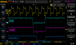
Works (just uses /DS, did still use a register to delay the falling /DSACK edge for inserting a wait state):

1722527028082.png

If you compare these, the /WE pulse is the same width. It's just shifted to the left by a half cycle in the top trace which I thought was good for adding more hold time considering I had more than enough setup time. The /DSACK pulse looks to be exactly the same too. The /WE pulse in the top trace meets Intel's timing requirements better than the pulse in the bottom trace, but the bottom one works and the top one doesn't.

The /DS solution is cleaner and simpler overall so it doesn't really bother me, but for my own understanding I just wish I knew what was going on. The only thing that jumps to mind is maybe the Intel flash timing specs I'm going off of are wrong. They seem in the same ballpark as the AMD specs though.
 
Last edited:

zigzagjoe

Well-known member
Yeah, at face value that looks fine to me..... Have you checked for timing interactions with /CS?
 

dougg3

Well-known member
Yeah, at face value that looks fine to me..... Have you checked for timing interactions with /CS?

The /CS pin on the flash chips is just tied to ground, so I shouldn't be hitting any problems there. Thanks for the idea though!

The only other thing that comes to mind is these N28F020 chips I got were from China (AliExpress and Utsource) so who knows about their quality. They appeared to be pulls from random other equipment like motherboard BIOS chips based on the data that was stored on them.
 

dougg3

Well-known member
I'm not sure if this explains any of the other issues I ran into earlier, but today after I threw together a simple LC PDS card with a few LEDs on it that I can control through the Mac's slot E address space, I came to the realization that with the LC PDS slot, I definitely always have to include /AS as part of the decision to respond. From the LC 475 dev note:

The /PDS.AS signal is not connected to the /CPU.AS signal. The /PDS.AS signal is used only for addresses in the slot $E address range; the /CPU.AS
signal is used for addresses in expansion slot and Super Slot spaces $6–$8, $A–$D, and $F (the slot $9 address spaces are used for built-in video circuitry).

/PDS.AS tells me whether it's really a slot E access or not, since I'm only looking at A31 and A24. Before I did this, I found that some other writes with A31=1 and A24=0 were happening too. I was super confused because one of my LEDs was turning off on its own after I turned it on, and I had no explanation for why.
 

zigzagjoe

Well-known member
Icky! I was thinking about making a LC slot version of my 30Video card, but all this nonsense they went through to make 68020 stuff work has me second guessing that! Still planning to do so, though.... the hardware is the easier part.

I'll tell you though, I'd really recommend looking at the ATF15xx line of CPLDs to make some of this tinkering easier. @halkyardo using one in his SEthernet design convinced me to give it a shot, and they're really quite amiable devices (5V native and ISP is nice too). Programming workflow is very similar - you can use (win)CUPL to do the logic, then use either ATMISP with the proper cable or use ATMISP to generate a SVF file a generic JTAG device can use to program.
 

dougg3

Well-known member
Icky! I was thinking about making a LC slot version of my 30Video card, but all this nonsense they went through to make 68020 stuff work has me second guessing that! Still planning to do so, though.... the hardware is the easier part.

I bet you won't have any trouble! I'm very new to this stuff so I think that's the main reason I keep running into snags.

I'll tell you though, I'd really recommend looking at the ATF15xx line of CPLDs to make some of this tinkering easier. @halkyardo using one in his SEthernet design convinced me to give it a shot, and they're really quite amiable devices (5V native and ISP is nice too). Programming workflow is very similar - you can use (win)CUPL to do the logic, then use either ATMISP with the proper cable or use ATMISP to generate a SVF file a generic JTAG device can use to program.

Definitely! I'm already sick of pulling the chip and putting it in a programmer over and over again. I even read that another option is you can use Intel/Altera's Quartus software to make a bitstream for the equivalent MAX7000 model and then use Microchip's POF2JED utility to convert it for the equivalent ATF15xx. That would allow using Verilog/VHDL.
 

dougg3

Well-known member
I don't know how to let things go!

Even though I'm probably fine on /WE rising edge hold time with my hardware since the ATF22V10 is so fast, I was curious about what I could have done to fix it if the timings really had mattered there. So I tried sticking with using /DS for the falling /WE edge (during S3) but passing it through two cascaded registers to time the rising edge using the clock (at the beginning of S4, after the wait cycle, and well before the /DS rising edge). That also works perfectly fine and gives me plenty of data hold time.

I'm kind of tempted to stick with that logic for more headroom because there are some stock Apple flash SIMMs, like the ones that have been observed in the set top boxes, that have more than 4 chips and thus have their own logic ICs that pass /OE and /WE onto the proper chips, adding further delay. I might have trouble with that hold time spec on them otherwise.

I played further with the timing of the /WE falling edge in order to understand why my earlier attempt failed. Here's what I discovered:
  • /WE falling edge at /AS falling edge in S1: fail
  • /WE falling edge at the start of S2: fail
  • /WE falling edge at /DS falling edge in S3: success
  • /WE falling edge at the start of S4: success
So it looks like if I try to drop /WE low before /DS, the Intel chip doesn't like it. This makes absolutely no sense based on all the timing diagrams I've been looking at, unless somehow the address isn't valid until around the time /DS goes low. And even so, it works fine with the AMD chips. Maybe Intel's spec sheet is wrong and it really does have some significant address setup time requirements. I don't know how else to logically explain what I'm seeing. Oh well, I seem to have a solution that works.
 
Top