-
Updated 2023-07-12: Hello, Guest! Welcome back, and be sure to check out this follow-up post about our outage a week or so ago.
You are using an out of date browser. It may not display this or other websites correctly.
You should upgrade or use an alternative browser.
You should upgrade or use an alternative browser.
ProtoCache1 - IIsi/SE/30 PowerCache Adapter Prototype Development
- Thread starter Trash80toHP_Mini
- Start date
Trash80toHP_Mini
NIGHT STALKER
Gotta do it, all the puzzle parts have to fit together between my ears. Did breaking it down to the number of traces involved work for you. With the buses all on the page at once it looks really complicated, but it's as simple as can be. Next up is modeling the reference card in Illustrator.
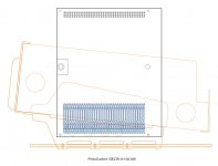
Should have remembered this one, it gives a good indication of the relationship of the card to the chassis deck.
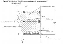
These two are from the page that's the gold standard of card design for the SE/30 in DCaDftMF3e:
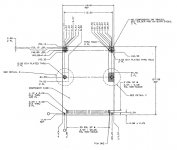
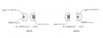
Overlaying the info on the largest sanctioned PDS card will be easy. I've always wondered about the top pair of mounting holes? Has anyone seen or heard about a frame that might use these seemingly redundant/impractical features? Lots of cards have the holes and my DayStar COLORCARD has them implemented EXACTLY as specified with the divits dutifully designed and in place.
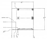
What the heck could be the purpose?
Anyhoo! What CAD file types can KiCAD import for the board shape, reference points and drill points for mounting holes and the MB connector in the diagrams above?
Should have remembered this one, it gives a good indication of the relationship of the card to the chassis deck.

These two are from the page that's the gold standard of card design for the SE/30 in DCaDftMF3e:


Overlaying the info on the largest sanctioned PDS card will be easy. I've always wondered about the top pair of mounting holes? Has anyone seen or heard about a frame that might use these seemingly redundant/impractical features? Lots of cards have the holes and my DayStar COLORCARD has them implemented EXACTLY as specified with the divits dutifully designed and in place.

What the heck could be the purpose?
Anyhoo! What CAD file types can KiCAD import for the board shape, reference points and drill points for mounting holes and the MB connector in the diagrams above?
Trash80toHP_Mini
NIGHT STALKER
Before I start this, I thought it would be a good time to ask for assistance. If anyone is an experienced mechanical CAD user, this would be a much appreciated contribution to the project. My experience is limited to creating a few designs back in the early nineties from scratch. It never included reading a mechanical drawing to input data as in this process.
I could do it in illustrator as a graphic for cutting a rubylith or silk screen stencil on my plotter, but those files would likely prove to be ineffectual for this purpose. Importing a CAD file format for use in Illustrator works in my graphic design process for laser printed etch resist film which was my original intent. However the precision drill file type data required for KiCAD or the like is lost in my process. Exporting the object oriented graphics as .DXF etc. from Illustrator (running them through Corel Draw for doing the translation) won't cut it for a KiCAD file import by PCB layout application for creating Gerber/drill file process boards.
TIA for any help.
< tangential TLDR mode >
It's a bit ironic that CAD files for PCB production were developed by Joseph Gerber and here's why:
In high school I considered myself a fine artist, so much so that when I went into full on stubborn mode when I took Art III and found out it was for commercial design. I sat at my table refusing to participate, accepting the fact that I would fail the course if I wasn't allowed to transfer to another elective. The very stubborn Daughters of Charity had met their match, relenting and allowing me to take Sociology for the balance of the semester. I never let on that they'd actually gotten the better of me because I'd rather have taken that F than sit through those classes, which I found to be the second most aggravating experience of high school and college put together. But that's another story. The sendoff the Vice Principal gave me was well and truly sweet. The last of the many things she'd said to me was "I hope you like what you do in college, because God help them if you don't!" [ ] ]'>
] ]'>
Somewhere in the process of taking enough fine arts electives (mostly printmaking) to qualify as a second major if there's been a degree program, I decided that I wasn't truly a fine artist after all. I loved the processes for every medium for making drawings, paintings, prints and sculptures. But not finding a "voice" to say anything of import (that's a bit ironic too) I decided that craftsmen (like my grandfathers) don't starve, they eat three square meals a day and make payments on a house. They offered me a "One Man Show" during final quarter before graduation and I took them up on it if they'd let my friend participate. By then I insisted to the faculty that I wasn't an artist, I was a craftsman and I wound up in the sign business. Not bad, on that path I beat my goal of owning my own screen printing business by age 30 by a couple of years.
I'd found the process apprenticship aggravating enough that I almost packed it in to take up a sales job at Burroughs that my Mechanical/Systems Engineer dad had lined up for me in September. While dejectedly sweeping the floor one day, I came to the realization that "The're gonna automate this sh*t!" 8-o So I stuck it out with dad's approval, finishing my apprenticeship at the company I'd wind up owning in NYC.
Enter Joseph Gerber/Gerber Scientific and the Signmaker III, the first mass produced vinyl letter cutting system. I waited it out until they offered the second generation "Sprint" which had a TTL display replacing the neolithic LED readouts of the III. When Gerber introduced a closed system for logo design based on a digitizing tablet, an Apple IIe and proprietary software I went into full on stubborn mode again until I sourced the MacSignMaker video to vinyl system. It was still proprietary software, but it didn't fully closed. Longer tangent short, I found myself using the Gerber Sprint to prototype an emulator/reader for Gerber's closed font format ($300 per typeface) and doing the large scale polyline plots that led us in breaking Gerber Scientific's proprietary font cartridge format. This let us import Type Three PostScript fonts created on the Mac in Fontographer into CorelDraw as "Readable Postscript." Those, long with CorelDraw's bundled fonts and any Type Three font available for DTP could be used in emulation mode with Gerber's proprietary machines. We did a translator for graphics exported from CorelDraw as the character "A" as well. This was the first "Postscript Translator" for producing signs and I was the only one doing it in the greater metropolitan area at the peak of the DTP revolution, beating Gerber Scientific and everyone else in the industry by a little over a year! But I'm now letting on that Gerber, like the nuns had, may have finally gotten the better of me.
Now I need to use Joseph's Gerber System Corp's file format for this, my second crazy reverse engineering/emulation electronics project. : At least this one's an open standard paper tape format for industrial use, long predating the SignMaker III. So maybe I'm still ahead of Gerber after all! :rambo:
If that you've read this drivel, I hope you've found it entertaining. Sweet irony, I'm definitely enjoying it!
< /tangent >
Little help?
I could do it in illustrator as a graphic for cutting a rubylith or silk screen stencil on my plotter, but those files would likely prove to be ineffectual for this purpose. Importing a CAD file format for use in Illustrator works in my graphic design process for laser printed etch resist film which was my original intent. However the precision drill file type data required for KiCAD or the like is lost in my process. Exporting the object oriented graphics as .DXF etc. from Illustrator (running them through Corel Draw for doing the translation) won't cut it for a KiCAD file import by PCB layout application for creating Gerber/drill file process boards.
TIA for any help.
< tangential TLDR mode >
It's a bit ironic that CAD files for PCB production were developed by Joseph Gerber and here's why:
In high school I considered myself a fine artist, so much so that when I went into full on stubborn mode when I took Art III and found out it was for commercial design. I sat at my table refusing to participate, accepting the fact that I would fail the course if I wasn't allowed to transfer to another elective. The very stubborn Daughters of Charity had met their match, relenting and allowing me to take Sociology for the balance of the semester. I never let on that they'd actually gotten the better of me because I'd rather have taken that F than sit through those classes, which I found to be the second most aggravating experience of high school and college put together. But that's another story. The sendoff the Vice Principal gave me was well and truly sweet. The last of the many things she'd said to me was "I hope you like what you do in college, because God help them if you don't!" [
Somewhere in the process of taking enough fine arts electives (mostly printmaking) to qualify as a second major if there's been a degree program, I decided that I wasn't truly a fine artist after all. I loved the processes for every medium for making drawings, paintings, prints and sculptures. But not finding a "voice" to say anything of import (that's a bit ironic too) I decided that craftsmen (like my grandfathers) don't starve, they eat three square meals a day and make payments on a house. They offered me a "One Man Show" during final quarter before graduation and I took them up on it if they'd let my friend participate. By then I insisted to the faculty that I wasn't an artist, I was a craftsman and I wound up in the sign business. Not bad, on that path I beat my goal of owning my own screen printing business by age 30 by a couple of years.
I'd found the process apprenticship aggravating enough that I almost packed it in to take up a sales job at Burroughs that my Mechanical/Systems Engineer dad had lined up for me in September. While dejectedly sweeping the floor one day, I came to the realization that "The're gonna automate this sh*t!" 8-o So I stuck it out with dad's approval, finishing my apprenticeship at the company I'd wind up owning in NYC.
Enter Joseph Gerber/Gerber Scientific and the Signmaker III, the first mass produced vinyl letter cutting system. I waited it out until they offered the second generation "Sprint" which had a TTL display replacing the neolithic LED readouts of the III. When Gerber introduced a closed system for logo design based on a digitizing tablet, an Apple IIe and proprietary software I went into full on stubborn mode again until I sourced the MacSignMaker video to vinyl system. It was still proprietary software, but it didn't fully closed. Longer tangent short, I found myself using the Gerber Sprint to prototype an emulator/reader for Gerber's closed font format ($300 per typeface) and doing the large scale polyline plots that led us in breaking Gerber Scientific's proprietary font cartridge format. This let us import Type Three PostScript fonts created on the Mac in Fontographer into CorelDraw as "Readable Postscript." Those, long with CorelDraw's bundled fonts and any Type Three font available for DTP could be used in emulation mode with Gerber's proprietary machines. We did a translator for graphics exported from CorelDraw as the character "A" as well. This was the first "Postscript Translator" for producing signs and I was the only one doing it in the greater metropolitan area at the peak of the DTP revolution, beating Gerber Scientific and everyone else in the industry by a little over a year! But I'm now letting on that Gerber, like the nuns had, may have finally gotten the better of me.
Now I need to use Joseph's Gerber System Corp's file format for this, my second crazy reverse engineering/emulation electronics project. :
If that you've read this drivel, I hope you've found it entertaining. Sweet irony, I'm definitely enjoying it!
< /tangent >
Little help?
Last edited by a moderator:
I have illustrator CS2 (even if I can't produce anything meaningful in it), which will open your Illustrator 8 files, and save it in a myriad of file formats. One has got to work, but I'll have to figure what that one is. BTW: Thanks for PDFing your illustrator files for viewing on the web. It retains its vector graphics element, while making it easy to view on my phone, or my computer without having to open any other program.Anyhoo! What CAD file types can KiCAD import for the board shape, reference points and drill points for mounting holes and the MB connector in the diagrams above?
I will probably do the drilling layout myself in PCBNew, KiCad's PCB layout program. Gerbers are always nice to have.
Board Shape is easy to do, and will take me all of 3 minutes to layout in PCBNew. Drilling points are easily added. KiCAD's PCB component footprint will layout the drilling holes for the connectors.
Funny how this all comes full circle :lol:
Trash80toHP_Mini
NIGHT STALKER
Sounds to me like now you're it in the production circle tag game. Building the board in KiCAD by inputting Apple's dimensions from origin (the rear mounting hole of the specified PDS EuroCard DIN connector) will be the way to go. You can export the file to me via CS2 for further playtime. I'll be dropping the angled cutoff in the DiiMO form factor and sticking to Apple's spec, minus the redundant mounting holes on top along with the rear hole.
You're the first to comment of the PDF attachments. I do them for myself for going over them at work in HiRes and printing details for markup during downtime.
Tag, you're it! [ ] ]'>
] ]'>
You're the first to comment of the PDF attachments. I do them for myself for going over them at work in HiRes and printing details for markup during downtime.
Tag, you're it! [
Trash80toHP_Mini
NIGHT STALKER
Attachments
Trash80toHP_Mini
NIGHT STALKER
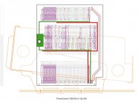
Looks like I'm about done. No wire wrap for power or ground which are in red and green, that's in copper. Board's within Apple Spec other than the missing mounting hole for the rear tab that's going to wind up in recycling. Much that side of the chassis of my incomplete SE/30 will be removed. I'll likely build a Plexi case with easy access, been wanting to do that, don't wanna hack up the /30 bucket or the VisiblePlus bucket I already did. Its side is too high for the wire wrap pins for the soldered MB connector. The setup without the chassis that I've been using for testing cards isn't up to this project.
IIRC, something like half a dozen control lines (Purple) and a couple of address lines (Yellow in the layered AI file) are involved in the active adaptation circuit. Anything heading through that (yet to be developed) setup will be in black and white wires. Data lines are a simple bus that'll be wrapped first in Brown wire because it doesn't change.
Dunno, time to think about things for a bit and line up info on pinouts. The modeling in AI8 was a lot of fun, but it's sorta garish when the Yellow and Brown aren't knocked back to gray. Thick traces are Component Side, thin traces are Solder/Wrap Side.
ProtoCache1-DELTA-A-102.PDF
Attachments
Trash80toHP_Mini
NIGHT STALKER
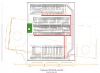
This one is Solder Side only. A few corrections need to be made to Row B of the MB connector, but it's pretty darn close to being finished.Do you need me to do the Component side?
Hopefully I can get the text in for the silk screen layer before too long and that you'll be able to import that into your layout. We'll be treating what's normally the Solder Side as the component side so the silk screen layer will be on the Wire Wrap side. Thank goodness the text can be tiny! Having all the pinout/signal info printed on the board for wire wrap prototyping will be incredibly helpful. The areas between the connectors and the wire wrap headers will remain free of rats nested wires. I'm not implementing thruholes/pads for P/G/n.c. which will make it even easier to keep everything straight while wrapping! [
What's easiest for you to import? Board outline and text together in .EPS .PDF or .AI8? I need to include the origin point now that I think of it. Maybe I should wait to see what you shoot back at me and I'll add the text to that?
ProtoCache1-EPSILON-A-000.PDF
Attachments
Trash80toHP_Mini
NIGHT STALKER
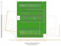
Little help please!
Testing 1.25mm Text. How well will this print on in SEEEDlike PCB process? Minimum type size is 1mm. Is the text imported and printed in a specified typeface at that size or is it imported as outlines/formatted text as in the case of a custom logo?
ProtoCache1-EPSILON-A-004.PDF
Attachments
Trash80toHP_Mini
NIGHT STALKER
What's the typeface look like? Have you got a link hand to a HiRes pic of a KiCAD output SEEED board? Is it possible to fit the text for the signals or will I be limited to Pin/Row information? It's easy enough for me to print paper labels to paste onto the board if needs be.
Trash80toHP_Mini
NIGHT STALKER
Interesting twist popped into focus in the ole noggin just before I stumbled out of bed to put up the coffee. May or may not want to drop the CI/PDS connectors and shorten the board by about 1cm. I realized I can buy 120 less long wire wrap header pins and simply substitute a second wire wrap Eurocard 120F connector in place of them for wrapping my connections to the RA PDS passthru slot on top of the PCB. It appears I've made provision for a second, zero footprint PDS expansion slot in the ProtoCache1 PCB spec after all. Just gotta make sure the card will clear the CRT.
edit: Duh! [:I] ]'>
edit: Duh! [:I] ]'>
Last edited by a moderator:
Trash80toHP_Mini
NIGHT STALKER
Attachments
Trash80toHP_Mini
NIGHT STALKER
Attachments
Trash80toHP_Mini
NIGHT STALKER
Pic may give a better notion of where I'm going with this:
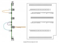
The blue loop and orange loops are the longest "traces" necessary to connect the most far flung signals crazily cris-crossing between MB->CI connectors and then CI->PDS connectors respectively.The rest of the wires will be of equal length and make up a rat's nest of meandered "traces."
I've interposed a 120 pin PCI slot connector that will have traces from the most probable signal suspects to one side of the edge card connector from the Motherboard and the other side leads to thruholes for headers. That gives me 60 lines up to the daughtercard and sixty lines back down again. Won't use but a handful, but PCI risers used for parts are super cheap on eBay from China. PCI connectors and SEEEDed 10cmx10cm protobards with edgecard teeth are a match made in geek heaven.
Taking the active adaptation playground off ProtoCard1 and onto a daughtercard plugged in topside makes a world of sense to me. I can wire up the passive setup on the 1U riser that donates its edgecard connector. May not even need to do any gating for multiple test setups, just pull one out, move the PAL to the next card setup and plug it in, with the passive card handy to make sure nothing's borked on the wire wrap side in between . . .
. . . lets me procrastinate a bit while I figure out what direction to take on that while getting wire wrapping under way for almost all the connections.
The purple wire transfers the down side signals to the CI slot. The length of traces running up one side and down the other of the adaptation daughtercard will be factored into the lengths of the blue and orange main bus loom. If a new signal comes into play, the long wire gets snipped, routed up the daughterboard and right back down again with length integrity preserved . . . maybe. :-/
Not exactly sure how this will work as yet, but it takes PCB estate pressure off ProtoCache1, KISS qualifies that board and transfers any complexity onto an inexpensive plug in protoboard or just a de-connectored PCI riser PCB wired up as a breadboard kinda deal.
Last edited by a moderator:
I like the idea of having a plug in active adaptor, at least for the moment. Eventually, we will pop on some SMD type PAL/GAL/CPLD to the card somewhere for it.
KiCad convininently already has a PCI slot in the its default parts library, so adding one to ProtoCard1 won't be very difficult.
The only problem I see is that now I have more through-hole connections to solder on it! [ ] ]'>
] ]'>
KiCad convininently already has a PCI slot in the its default parts library, so adding one to ProtoCard1 won't be very difficult.
The only problem I see is that now I have more through-hole connections to solder on it! [
Trash80toHP_Mini
NIGHT STALKER
Keep It Simple Stoopid! :I
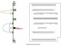
How about just 40 thruholes? First pass at the adaptive daughtercard notion was the work I did for Project CheeseBall which was easy to import into a tangential AI8 file. Couldn't find a wire wrap version of the PCI slot connector last night and in between alarms this morning snoozemares of desoldering PCI crap from the UtzJar made me think of my OrangePi and RPi prototyping goodies that are even less expensive and much handier than PCI risers.
Keeping the total length of the magenta circuit wires/traces to the blue/orange bus wires will be a PITA, but the daughtercard as pictured is KISS compliant once more.
Only worries then were capacitance/whatever that adding connectors to the circuit causes . . . which popped load limits of 030 PDS signals into the mix . . . which made me realize why DayStar/DiiMO et al limited passthru provision to a single connector . . . which put buffers/line drivers into the reserved prototyping area . . . which threw ProtoCache1 out of KISS compliance yet again . . . which snoozemare got me up and out of bed when the alarm went off again . . .
No good thought goes unpunished. :-/
Last edited by a moderator:
Trash80toHP_Mini
NIGHT STALKER
KISS! [ ] ]'>
] ]'>
Gotta do something different for a few days. The tug of war between visions of Paladin reassembly and ProtoCache1 development seems like the battle of Midway has been raging between my ears.
Scratch two Centimeters! [ ] ]'>
] ]'>
Dropped the original design config for Wire Wrap to Soldertail Connector conversion for the board. Went back to wire wrap for the passthru to simplify/cheapify ProtoCache1. I've got the two "NuBus" EuroDIN96RA connectors already modified/melded and sitting in the PDS of the SE/30 per pic in the IP, doing same to a pair of female connectors at the top end poses no challenge.
Time for cost analysis of what's suddenly a 14cm x 13cm PCB. [ ] ]'>
] ]'>
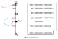
If I can't find RA Female Wire Wrap Connectors, now I know the PDS VidCard will definitely clear the CRT and the straight up version of the 96 pin "NuBus" wire wrap part is available at $6.05 ea. from DigiKey.
In my searches I've found 120 pin PDS connectors closer to that price range for the production release of the adapter, so that shaves a pretty penny off total cost.
Gotta do something different for a few days. The tug of war between visions of Paladin reassembly and ProtoCache1 development seems like the battle of Midway has been raging between my ears.
Scratch two Centimeters! [
Dropped the original design config for Wire Wrap to Soldertail Connector conversion for the board. Went back to wire wrap for the passthru to simplify/cheapify ProtoCache1. I've got the two "NuBus" EuroDIN96RA connectors already modified/melded and sitting in the PDS of the SE/30 per pic in the IP, doing same to a pair of female connectors at the top end poses no challenge.
Time for cost analysis of what's suddenly a 14cm x 13cm PCB. [

If I can't find RA Female Wire Wrap Connectors, now I know the PDS VidCard will definitely clear the CRT and the straight up version of the 96 pin "NuBus" wire wrap part is available at $6.05 ea. from DigiKey.
In my searches I've found 120 pin PDS connectors closer to that price range for the production release of the adapter, so that shaves a pretty penny off total cost.
Trash80toHP_Mini
NIGHT STALKER
Barely laid sown to clear my head and whack! 8-o
Scratch 2 Centimeters! (four Flattops total)
Reduced the now redundant "prototyping area" and the board's now 12cm high and 13cm wide.
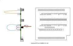
edit: I'll probably increase width to 14CM for elbow room, but PCB cost should be down, we'll see by how much.
Scratch 2 Centimeters! (four Flattops total)
Reduced the now redundant "prototyping area" and the board's now 12cm high and 13cm wide.

edit: I'll probably increase width to 14CM for elbow room, but PCB cost should be down, we'll see by how much.
Last edited by a moderator:
Similar threads
- Replies
- 70
- Views
- 5K
- Replies
- 67
- Views
- 4K
- Replies
- 25
- Views
- 3K
- Replies
- 9
- Views
- 2K
- Replies
- 0
- Views
- 738

