• Updated 2023-07-12: Hello, Guest! Welcome back, and be sure to check out this follow-up post about our outage a week or so ago.

Project30 - IIsi NuBus Adapter in SE/30 - fifth edition

Trash80toHP_Mini

NIGHT STALKER
@max1zzz thanks so much for the layers of your IIcx Redux.

I've reconstructed the traces/chips/pads for the three signals that meander down off NUCHIP in the NuBus section of the Bomarc Schematic.
Trying to figure out where ARST, LO0 and HI0 go and what they are doing?
Some of the circuit seems like it can be recreated on the NuBus Adapter side of the PDS?

Red = Solder Side Traces
Blue = Component Side Traces
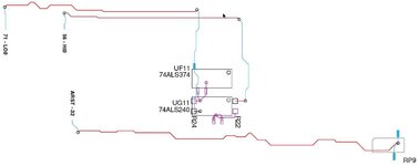

WTF.jpgStrange:
HI0 and LO0 are jumbled into multiple pins on one side or the other of resistors on the solder side?
ARST is connected to a pair of pins on a resistor pack?

How much deeper do you think I need to dive into this?
Next step would seem to be scouring the remainder of the pages for the ICs to see what might be up?
 

Melkhior

Well-known member
Trying to figure out where ARST, LO0 and HI0 go and what they are doing?
ARST is probably an asynchronous reset.

HI0 and LO0 are probably clocks. In the IIcx schematics (bomarc) page 4, two crystals (Y2, Y3) are fed into UG11, with multiple drivers in parallel, presumably because clocks have large fan-outs (lots of users) and are long-distance.

IT seems to me UF11 does some divide-by-2 from LO0 (~32 MHz from Y2) to produce the ~16 MHz clock for the system. HI0 is 40 MHz from Y3.
 

Trash80toHP_Mini

NIGHT STALKER
Thanks, do my AI doodles help, not so good with words.

IT seems to me UF11 does some divide-by-2 from LO0 (~32 MHz from Y2) to produce the ~16 MHz clock for the system. HI0 is 40 MHz from Y3
On the expansion card PDS provides CPUCLK and the C16M reference clock for dedicated use on expansion cards = No problem?

40 MHz crystal can is in spec for the Expansion Card. Does UF11 need to be added for synchronizing the two clocks or does is decouple them for asynchronous state in NUCHIP? Can such shenanigans be accomplished upstream of PDS on the card?

My guess is that such is possible and that the three reserved pins were intended to feed the three Via connections to NUCHIP on a NuBus adapter?

Theory there would be reserved pin provision for a future Mac II variant, never implemented. Apple changed memory addressing setup you detailed upthread and updated NUCHIP30 was designed to run on the PDS w/o the VIA connections?

ARST remains a mystery then? I'll fan out the traces from RP9 to see where thy lead with annotations on any ICs involved.
 

Melkhior

Well-known member
On the expansion card PDS provides CPUCLK and the C16M reference clock for dedicated use on expansion cards = No problem?
Good question. The NuChip30 in the IIci seems to be only fed two clocks - a 40 Mhz signal (presumably to generate the 25/75% duty cycle NuBus clock @ 10 MHz, from Y7) and the system clock. That last one comes from the MDU and is also fed to the CPU and FPU, and is presumably synthesized from the 50 MHz Y6.

But the NuChip in the IIcx is fed three clocks - LO0, HI0, an the CPU clock itself ('CK', pin 68). HI0 can be generated locally, CK is CPUCLK on the PDS. But LO0 isn't readily available. It might be possible to regenerate it from the CPUCLK using some form of PLL or similar, but it will likely change the phase relationship with the CPUCLK... for that kind of stuff I really don't know what to do.
 

Trash80toHP_Mini

NIGHT STALKER
Great , , , just maybe. Let me guess, LO0 would be the clock eliminated as a NuChip30 input? Thanks again for your help.

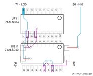
LO0 would seem be generated in UG11 and UF11 it would seem? I guess it would be my next step to doink in all inputs and outputs from that mess to see if their innards lead anywhere else off chip.

Someone around here ought to be able to figure out those phase relationships for generating LO0 from PDS inputs?.

Paging @trag and company! :unsure:
 

Trash80toHP_Mini

NIGHT STALKER
Another way to look at this?
NuChip was developed for the revised Macintosh II, replacing the discrete logic NuBus controller in first release Macintosh II.

As such, its origin was the 68020 architecture. It was adapted/kluged into the stopgap 68030 II/IIcx architecture.
NuChip30 was likely in development at the time for the Macintosh IIci with its new memory architecture and Onboard Video?

Time to look for the Macintosh II schematic I think. As it's from the NuChip version, comparisons might be helpful?
 

Trash80toHP_Mini

NIGHT STALKER
OK, I was remembering when @Melkhior had said that NuChip30 was developed for 68030 systems up thread. Turned out not to have been the case, looks like NuChip30 along with MDU for the IIci and for use in the IIfx. NuChip30 supported 20/25/40MHz 68030 systems, after that they went to NuChip33 I think?

Head's fuzzy, at home getting over a stomach bug today. Took a look at the pinout and symbology for the 240 and my head imploded. :oops:
But managed do a detail if anyone wants to fill in the voids.

UF11-UG11_Detail.jpg
 

Attachments

  • UF11-UG11_Detail.pdf
    17.9 KB · Views: 1
Top