• Updated 2023-07-12: Hello, Guest! Welcome back, and be sure to check out this follow-up post about our outage a week or so ago.

Project30 - IIsi NuBus Adapter in SE/30 - fifth edition

Trash80toHP_Mini

NIGHT STALKER
Again: re-iterating the recommendation to start small and scale from there. There's no need to hijack $E. @Melkhior and @Phipli have established a good case for basic interface compatibility with minimal glue logic, so try to get your chipset working and a single slot before you worry about more.
Such suggestions would be why I'm positing all my insanity in this rev. of the project series. That's an I approach I could never thought of as it's beyond my ken. Such would probably not have popped up but for my fascination with hacking about woth $E.
 
Last edited:

Trash80toHP_Mini

NIGHT STALKER
If you pull the video ROM, you're doing the equivalent of pulling the declrom on a PDS card. If you write to the address space that the card occupies, it still gets the reads and writes regardless of whether the ROM is there or not.
Suffice it so say: HUH??? :oops:

Again, well beyond my understanding at present, but should be easily verified with a logic analyzer if that's the case. Doesn't seem a possibility if Slot Manager doesn't know anything is there. Especially as the drivers are in DeclROM for all the cards I've played with. Drivers for an Ethernet card loaded at startup would be another case entirely I'd think?
 

cheesestraws

Well-known member
Again, well beyond my understanding at present, but should be easily verified with a logic analyzer if that's the case

I promise you this is the case. Address decoding happens whether or not the slot manager knows about the card. Address decoding is done in hardware I have personally loaded drivers for PDS cards from disc. A DRVR loaded from a declrom is not special at all, it's just another DRVR loaded early in the startup process.
 

Phipli

Well-known member
If the Video ROM is pulled, there is no video hardware in that machine state for system software to try to handle as it no longer exists in mapped memory at startup, no?
Its still physically there.

Removing a phone number from your address book doesn't stop the phone number for that phone working.
 

Trash80toHP_Mini

NIGHT STALKER
I'll accept that as gospel then, guys. Thanks!

Gotta play with form factors for the Prototype board next. It'll likely have provision for a daughtercard or prototyping area for glue to address a second slot per the method suggested above. Alternately it'll be jumpered to occupy one of the PDS Slot assignments?

8vRuFk.jpg

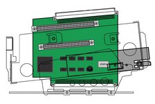
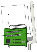
Physically, I'm seeing the primary slot positioned in the lower NIC's position atop the ZIP,/HDD placeholder. Such leaves enough cubic for the PowerCache Card above it, roughly in the AAUI card's position and a passthru slot above for the elusive Grayscale Card in max SE/30 PDS card spec. Second NuBus slot would be underneath, occupying HDD cubic if the building blocks work out the way I'm seeing them at present.

Dunno, need a nap. Today is Sunday in my time zone. :sleep:
 
Last edited:

Melkhior

Well-known member
Suffice it so say: HUH??? :oops:
Hardware addressing is quite simple, it's just comparison to known values.

Basically, each piece of hardware is assigned a range of addresses from the 2^32 valid addresses (32 bits), listed in the 'memory mao' (i.e., how the memory map to different functions). For NuBus that's the slot area and superslot area.

Each piece of hardware then compare every address outputed by the CPU against its own range, and if there's a match, react to it. For instance, in the IIsiFPGA the relevant hardware definition is:
Code:
        # selection logic
        my_slot_space = Signal()
        self.comb += [ my_slot_space.eq((A_i[24:32] == 0xf9)) ] # fixme: abstract slot $9
If the upper 8 bits of the address are 0xF9, then we're in the PDS pseudo-slot area. The signal 'my_slot_space' is asserted, and the device will react to it appropriately. There's similar code in the NuBusFPGA comparing the address to a SlotID instead of hardwiring the $9.

The video subsystem in the SE/30 likely does something similar, but for 0xE / $E. It doesn't matter *why* the CPU accesses somewhere in this range of addresses, if it does, then the hardware *will* answer.

The CPU itself has no knowledge of that - it just spits addresses (the 68k was a sort of pioneer for doing everything 'memory mapped', rather than use dedicated I/O operations). The software must be aware of the 'memory map' to deal with it properly. In Macintoshes, the Slot Manager (in the ROM) looks for Declaration Rom in specific addresses of the slot area, and handle what it finds. If you remove the Declaration Rom, it doesn't know there's something there, but the hardware it still present and active and will still answer requests to the address range it 'owns'.

If some other hardware also answers to the same range of addresses... things will go very, very wrong. Do not do that.
 

Phipli

Well-known member
I'll accept that as gospel then, guys. Thanks!

Gotta play with form factors for the Prototype board next. It'll likely have provision for a daughtercard or prototyping area for glue to address a second slot per the method suggested above. Alternately it'll be jumpered to occupy one of the PDS Slot assignments?

View attachment 59758

Physically, I'm seeing the primary slot positioned in the lower NIC's position atop the ZIP,/HDD placeholder. Such leaves enough cubic for the PowerCache Card above it, roughly in the AAUI card's position and a passthru slot above for the elusive Grayscale Card in max SE/30 PDS card spec. Second NuBus slot would be underneath, occupying HDD cubic if the building blocks work out the way I'm seeing them at present.

Dunno, need a nap. Today is Sunday in my time zone. :sleep:
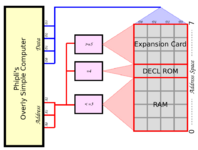
I drew this to explain so you can understand for the future. The address (and data) lines are hardware - they're just a matter of fact. The slot identifiers are addresses - they refer to specific locations in memory. The Decl ROM is at one location - the computer knows to look there to get information about the card and potentially code. Separately to that, the card is also wired into memory. If you remove the Decl ROM it frees up the space the Decl ROM used - but the card is still there in the memory map. writing to the cards memory range (E) will still be writing to the card. If you fit a second card in slot E, you're writing to both of them at the same time and confusing things because you're sending random and likely invalid commands to arbitrary places in the card's memory.

Does the following help? Imagine you're trying to overlay a second expansion card in the same memory 5, 6 and 7 in the address space. Both of them receive anything written to 5, 6 and 7. Both of them try to react to it. By removing the Decl ROM, you have only freed up address "4". Nothing else.

Yes, my imaginary computer only has 4 bytes of memory, arranged in 4 bit words. I didn't say it was a very good computer.

1690280183647.png
 
Last edited:

Trash80toHP_Mini

NIGHT STALKER
Cool, a lot to read-n-grok, thanks guys. Love that graphic especially. That's the way I learn/think, words are supplemental.

Meanwhile, I found enough of the old AI drawings and templates to get started. Dunno If there is even enough real estate available for a second slot, but I'll make a place for it if possible.
 

Trash80toHP_Mini

NIGHT STALKER
Played about in AI8 on the Lombard today. Looks like a single slot hacked onto the DiiMO adapter from @Bolle is the way to go for now. Spacing complications due to placement of the chassis mounting ears and card separation spec requirements make for a pain in the butt.

Have I left out any components? NuCHIP/Transceivers/Clock were all I could think of offhand.
P30-Single-Slot-000.jpg
Something seems amiss. I've got connectors at 5 degrees from PDS. Is the passthru parallel to the deck/FDD/HDD tops?

Is the P33 component side up or down on the adapter? Flipping it over and moving it as far back as possible frees up some real estate/cubic I think? Can almost certainly stagger a pair of slots for a shorter card aligned with the left ear and a longer card below it or some such.

3.5" SCSI HDD mounts vertically alongside the PSU box per one of the GAMBA arrangements.
 
Last edited:

Trash80toHP_Mini

NIGHT STALKER
If I might offer advice, you are suffering from a bad case of scope creep.... get a functional proof of concept first, then see about iterating to add more functionality rather than try to do everything in one fell swoop. Otherwise, projects tend to never get off the ground.
That's exactly what I'm going to do, KISS. @Melkhior and @Phipli have confirmed that the concept "should work" so here goes.

The above is not scope creep, it's an exploration of the possibilities for future insanity whilst bringing my drawings from a completed project. @Bolle and @joethezombie jumped in and brought that one to fruition. I have the the illustrations from that DiiMO form factor PowerCache Adapter as a starting point. So now it's time to knock it back to a simple prototype that'll be worth keeping around just 'cause.

In the drawing above, the slots are pointing at the back end of the case which requires flipping the bus around. Not gonna happen as it's a see monkey do exercise in manual board layout. The NuBus slot(s) will be oriented in reverse as compared the pic of my cubic experimentation.

I will however be extending the bus to that second slot per IIcx for experimental insanity's sake, almost KISS compliance. :p
 

Trash80toHP_Mini

NIGHT STALKER
New question: NuBus and PDS passthru will be split into a V configuration, so should the slot be terminated per RP1-4 on that side of the fork?

IIcx-NuBus-Implementation-00.jpg

TopIIcxMaxx-01.jpg
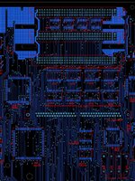
I've got the bottom side of my board and the topside traces thanks to @max1zzz for see-monkey-do routing in AI. Only serious complication will be repositioning NUCHIP to the area occupied by FPU, but not really a big deal.

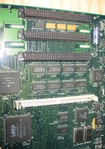
I've got the IIsi adapter for cribbing the NuBus subsystem's connection to PDS. Only deal there is the transceiver form factor. Wondering if I should just go ahead and replace the eight chip 651 net with the available 74ACT16651 2 chip net during the process? KISS principal says no, more adventurous leaning says go.

Whatcha think of the approach so far?
 
Last edited:

Trash80toHP_Mini

NIGHT STALKER
Thanks, not quite, but I found a couple of interesting tidbits tonight during downtime at work:

I think this might be the right size, less the four corner pins it should be a match?

Aim here is to solder the NuCHIP (from my IIcx or another donor) to that SMT->PGA adapter which can be socketed onto any of a progression of prototypes if needs be. After that's done I can send it back into my IIcx unless @trag comes up with a donor NuCHIP from one of the IIcx boards with which he's planning to populate his Black SE/30 boards. HINT!!!!! ;)

I post pics and pdfs over at tinkerdifferent because I can't open anything up here to print out or examine without the major no-no of logging in here when I'm online in downtime at work. 😕
 
Last edited:

Trash80toHP_Mini

NIGHT STALKER
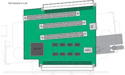
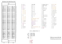
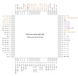
Just froze form factor development and outlined my NUCHIP pinout development roadblocks Project30_v6

P30-NuChip-pinout-dev-62.jpg.jpg

Had hoped patching the three reserved pins to VIA2 would be enough, no such luck. Might be at a dead end for this one given the UG11 connections. Does UG11 even exist on the SE/30 board? Haven't found it on my @Bolle reloaded board as yet. :(

And WTHeck are those red lines?
 
Last edited:

Chopsticks

Well-known member
Thanks, not quite, but I found a couple of interesting tidbits tonight during downtime at work:

I think this might be the right size, less the four corner pins it should be a match?

Aim here is to solder the NuCHIP (from my IIcx or another donor) to that SMT->PGA adapter which can be socketed onto any of a progression of prototypes if needs be. After that's done I can send it back into my IIcx unless @trag comes up with a donor NuCHIP from one of the IIcx boards with which he's planning to populate his Black SE/30 boards. HINT!!!!! ;)

I post pics and pdfs over at tinkerdifferent because I can't open anything up here to print out or examine without the major no-no of logging in here when I'm online in downtime at work. 😕
Oh ok, sorry I must have missed the need to solder to a carrier board. Just wondering and sorry if I missed it if you’ve already explained it but how come you need to solder the chip onto a pga adaptor rather then just use a socket, at least for prototype verification? Is it to do with clearance issues or am I just way off?

Black SE/30 boards… NuCHIP…. sounds like something exciting is in the works there
 

Trash80toHP_Mini

NIGHT STALKER
As I'd said, if I solder the NuCHIP (from my IIcx or another donor) to that SMT->PGA adapter it can be socketed onto any of a progression of prototypes.

Guess is that I've been barking up a very interesting, but wrong tree. Given the problems outlined on that NUCHIP pinout file I posted today it's not looking so good. Waiting to hear what @Melkhior and @Phipli have to say.

Just got the PDF of the IC to work!
NUCHIP-pinout-62.jpg
 

Attachments

  • P30-Nuchip-pinout-062.pdf
    46.4 KB · Views: 1
Last edited:
Top