• Updated 2023-07-12: Hello, Guest! Welcome back, and be sure to check out this follow-up post about our outage a week or so ago.

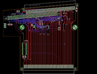
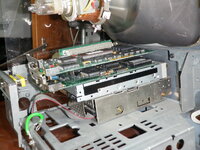
Project30 - IIsi NuBus Adapter in SE/30 - fifth edition

Trash80toHP_Mini

NIGHT STALKER
Back to basics: forever project reboot.

New approach is to take the IIsi NuBus Adapter on a trip back in time. It now seems to me that it's likely that NuChip30 may be the problem.

Nuchip ASIC replaced the discrete component implementation in the early release Macintosh II, supporting 16MHz clock of the series
NuChip 30 ASIC development required for support of the faster 25MHz IIci and 20MHz IIsi clocks in that generation of series.
____ NuChip 33 developed for support of later machines.

Hardware/firmware backward compatibility with earlier, slower NuBus machines would be unnecessary.

Given:
Macintosh SE/30 was a reduced form factor, PDS substitution (upgrade?) of the IIcx NuBus (NuChip) architecture.

Theory:
NuBus implementation of IIci/IIcx generation burned bridge of hardware/firmware implementation in earlier machines?

WAG:
Replacement of NuChip 30 controller on the IIsi NuBus adapter with NuChip from II/IIx/IIcx is worth a shot?
Such may rebuild the burned NuBus bridge to SE/30?

Assumption:
NuBus controllers would be agnostic in terms of transceiver implementation support?

Thoughts?
 
Last edited:

Melkhior

Well-known member
Thoughts?

There's two primary differences between the 68020 in the Mac II for which the NuChip was designed, and the 68030 in the newer systems.
(a) addition of the synchronous bus cycle (terminated by /STERM and optionally burst with /CBREQ and /CBACK, vs. the asynchronous cycle terminated by /DSACK)
(b) integration of the PMMU (the '020 uses an external PMMU, the '030 has one builtin

You can see the second difference in the Bomarc schematic for the II and IIcx - a bunch of signals going to the PMMU in the II are tied high or low in the IIcx. That should be a non-issue in practice, simply following Apple's lead should be enough. The NuChip30 doesn't seem to have those signals, understandably.

For the first difference, it's explicitly mentioned in the DCDMF3 for the PDS in the SE/30 and IIsi. A PDS device doing bus mastering in a SE/30 must deal with the memory controller using asynchronous bus cycle (/DSACK), whereas in the IIsi the memory controller uses synchronous cycle (/STERM). When a NuBus device does a bus master cycle, the NuChip will have to talk to the memory controller, and understand the appropriate type of cycle. If the NuChip30 only understands synchronous cycle, then it won't talk to the SE/30 memory controller - but it is connected to /DSACK in addition to /STERM... The original NuChip must understand asynchronous cycle, as that was the only type available with a '020, it's not even connected to /STERM.

So far so good.

However, there's another difference in the schematics, which is system-related and not CPU-related. In the IIci w/ a NuChip30, all connections from the NuChip I was able to understand - they go to the CPU, the dedicated drivers (343S1027), discrete drivers (74ALS240A, 74F244), a signal to the GLU for NuChip selection, ... Also, the interrupt lines from the NuBus slots are going to the RBV, which include the functions of the VIAs in previous Macs. Those signals are available on way or another in the SE/30 and IIsi PDS.

But in the IIcx, things are a bit different. The NuChip has three signals going to the VIA2 (to 2PB1, 2PB4, 2PB5). At first I thought they were forwarding the interrupts from the slots, but no - the interrupt lines from the slots go to 2PA0, 2PA1 and 2PA2 according to the schematics, also in VIA2. And the schematics say those are also connected to the GLU. My guess is that for those last three, one could substitute connectivity to the IRQ in the PDS slot, but I have no idea what are the NuChip <-> VIA2 connections for or how to handle them in relationship to the PDS. It's possible examining the ROM would give a clue as to their purpose...
 

Phipli

Well-known member
But in the IIcx, things are a bit different. The NuChip has three signals going to the VIA2 (to 2PB1, 2PB4, 2PB5). At first I thought they were forwarding the interrupts from the slots, but no - the interrupt lines from the slots go to 2PA0, 2PA1 and 2PA2 according to the schematics, also in VIA2. And the schematics say those are also connected to the GLU. My guess is that for those last three, one could substitute connectivity to the IRQ in the PDS slot, but I have no idea what are the NuChip <-> VIA2 connections for or how to handle them in relationship to the PDS. It's possible examining the ROM would give a clue as to their purpose...
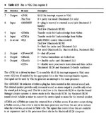
I misread part of your message, but am leaving the following here because it clarifies what you already said about how the interrupts are connected. It does show what Port B 1, 4 & 5 are though.

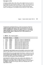
The hardware reference says "VIA2 (or the corresponding custom IC) supports features not present in one-
VIA Macintosh computers, such as interrupts from expansion cards, interrupts from the
Apple Sound Chip, and other features.
"

Note it also shows all six Nubus interrupts going to VIA2 port A like you said. This is on all Mac IIs of the era (IIsi wasn't released at the time, but was based on the IIci chipset).

VIA2 functions listed here :

Screenshot_20230719_100947_Drive.jpg

Screenshot_20230719_101053_Drive.jpg
 
Last edited:

Phipli

Well-known member
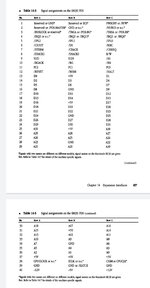
PDS pinout shows IRQ1, 2 & 3 present on the SE/30 PDS. I assume these are then wired into VIA2. This would be verifiable on the schematics for the SE/30 but I don't have them to hand.

I wonder what Pin C2 is? /TM0A and /TM1A are there. So is NUBUS "BusLk"?

Screenshot_20230719_102414_Drive.jpg
 
Last edited:

Melkhior

Well-known member
The hardware reference says "VIA2 (or the corresponding custom IC) supports features not present in one-
VIA Macintosh computers, such as interrupts from expansion cards, interrupts from the
Apple Sound Chip, and other features.
"

Oh, excellent catch! The IIci's NuChip030 has three pins connected to the RBV that I forgot about :-( Odds are, they are the TM0/TM1/BucLock signals that were carried by 2PB4/5/1 in previous implementations. Unlike the IRQs, those signals are synchronous, so the NuChip (of either flavor) might simply carry them from the NuBus to the CPU clock domain, where the asynchronous IRQs can be hooked directly to the VIA.

I remember (partial?) schematics of the SE/30 being available, it's likely worth checking where the BusLock/TM0/TM1 are going (or do a continuity testing on a real board). If it's to the same B register pins as in II systems, then it's likely the regular NuChip would connect to those signals directly. ... actually there's Kicad schematics from the whole motherboard, and it seems indeed those pins are just breakout of the VIA2 signals.

Another thing to check is if the 3 relevant pins (13, 31, 72 in Bomarc IIci) from the NuChip30 in a 'real' IIsi NuBus adapter are going to those 3 PDS pins directly - unfortunately I don't own one, and it cannot be confirmed from the pictures I've seen.
 

Phipli

Well-known member
On a IIsi NuBus riser...

13 is... A3 (PDS BusLock)
31 is... C3 (PDS TM1L0A)
72 is... a lot of counting... B3 (PDS TM1A)

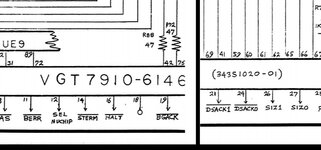
Pin C2 is connected to.... Pin 12 of the NuBus chip. Haven't checked the chip pinout sorry, so I don't know what that pin's function is.

Edit - The bromarc IIci schematic shows the same chip as the riser (343S1020-01). The pin is a select line "SEL NuChip"

Screenshot_20230719_121327.jpg

Hope this helps @Melkhior
 
Last edited:

Melkhior

Well-known member
On a IIsi NuBus riser...
13 is... A3 (PDS BusLock)
31 is... C3 (PDS TM1L0A)
72 is... a lot of counting... B3 (PDS TM1A)
Pin C2 is connected to.... Pin 12 of the NuBus chip. Haven't checked the chip pinout sorry, so I don't know what that pin's function is.
Edit - The bromarc IIci schematic shows the same chip as the riser (343S1020-01). The pin is a select line "SEL NuChip"
C2 in the PDS is /NUBUS, the NuBus selection signal - actually it just means 'address somewhere in $6000_0000 to$FFFF_FFFF', the entire expansion I/O range (including e.g. the internal video on a IIsi).

That confirms that the regular NuChip should be usable in a SE/30, all the required signals seem to be present. Thanks @Phipli for checking on the adapter.

The weird things is that AFAICT, the NuChip30 should work in a SE/30 as well, potentially excluding DMA bus mastering from a NuBus device if the NuChip30 can only understands /STERM as response to its requests. But 'slave-only' device _should_ work. @Trash80toHP_Mini, is bus-mastering the problem you're trying to solve? Or is it something else?
 

Phipli

Well-known member
C2 in the PDS is /NUBUS, the NuBus selection signal - actually it just means 'address somewhere in $6000_0000 to$FFFF_FFFF', the entire expansion I/O range (including e.g. the internal video on a IIsi).

That confirms that the regular NuChip should be usable in a SE/30, all the required signals seem to be present. Thanks @Phipli for checking on the adapter.

The weird things is that AFAICT, the NuChip30 should work in a SE/30 as well, potentially excluding DMA bus mastering from a NuBus device if the NuChip30 can only understands /STERM as response to its requests. But 'slave-only' device _should_ work. @Trash80toHP_Mini, is bus-mastering the problem you're trying to solve? Or is it something else?
I think I remember Bolle saying there are timing differences between the IIsi and SE/30... was it due to some signals being buffered? I forget.

I'm pretty sure this has been covered before.
 

Trash80toHP_Mini

NIGHT STALKER
System clock is the problem I think, the Radius IIsi NuBus adapter "just works" in the SE/30. But the NuBus clock is derived from the IIsi 20MHz clock, yielding only 8MHz in the SE/30 on aits 16MHz clock.

Looks like I've a bit of reading to do here, thanks guys.
 

Trash80toHP_Mini

NIGHT STALKER
That confirms that the regular NuChip should be usable in a SE/30, all the required signals seem to be present. Thanks @Phipli for checking on the adapter.
Fabulous! Did pinouts remain the same in the transition from NuChip to NuChip30?

The weird things is that AFAICT, the NuChip30 should work in a SE/30 as well, potentially excluding DMA bus mastering from a NuBus device if the NuChip30 can only understands /STERM as response to its requests. But 'slave-only' device _should_ work. @Trash80toHP_Mini, is bus-mastering the problem you're trying to solve? Or is it something else?
Just looking for an approach that might work. The signal issues you guys are talking about are way above my pay grade. I study the Block Diagrams looking for chinks in the different architectures armor to exploit. Then I muddle through the docs as best I can.

@trag is looking to populate his new SE/30 board(s) with components from his stack of surplus IIcx boards. That leaves NuChip sitting on those IIcx donor board(s). As the SE/30 is a modified IIcx board, that got me thinking about firmware/architecture and the possibility of ASIC swapping on the IIsi adapter for experimental purposes.

NuChip supply would be very limited and a new PCB/PDS Card would be required for the SE/30 form factor with PDS passthru provision.

Radius' discrete component adapter would be my choice as the starting point for a production board. Grafting the NuBus clock crystal into its schematic would be the heart of that project. Again, such things are way above my humble pay grade. 😞


edit: @Bolle have you done the schematic of the Radius adapter?
 
Last edited:

Trash80toHP_Mini

NIGHT STALKER
Nap, I've been looking for a solution for the fun of it. Started looking into this well before posting about it six and a half years ago. That was before I even had my first working SE/30 I think? Started out taking IIsi performance to the max as the SE/30's bane.
 

Melkhior

Well-known member
Fabulous! Did pinouts remain the same in the transition from NuChip to NuChip30?
Emphatically no. It's a complete redesign, at least externally. Which means you would need to restart a PCB design from scratch, there's no way to reuse the existing PCB with the different chip. Sorry for the bad news.

Radius' discrete component adapter would be my choice as the starting point for a production board. Grafting the NuBus clock crystal into its schematic would be the heart of that project.
Recreating a discrete version might indeed be easier, provided the chip have modern equivalent/are still available. It would also require extracting the content of whatever GALs/PALs are in there, I suppose. Those have modern replacement as I understand it (never tried PALs/GALs, because I could never figure out what modern hardware/software could program them... manufacturers seem to actively prevent you from using their chips by hiding that information or only having super-expensive solutions ?!?). NuChip are as you said very difficult to source.

Anyway I've thought about a couple 'alternate' solutions, but so far they don't fit the IIsi PDS adapter form factor:
(a) 'inline' FPGA
(b) 'offline' FPGA
(what can I say, I have a thing for FPGAs :) )

For (a) basically I'd just put a FPGA between the PDS and the NuBus. On the upside, gateware-wise, most of what is needed already work in the NuBusFPGA and IIsiFPGA. On the downside, it would require a lot of level-shifting chips that takes space and money, and a FPGA with _lots_ of I/Os. And that means a big FPGA with picky power requirements, probably using a BGA package, and that's a lot of complexity for the PCB. Best solution I've found so far is a LCMXO3LF-1300C-5BG256C, and that would likely require a double-sided 6-layers PCB, so not cheap.

For (b), basically that's just using discrete buffers/drivers like a IIcx and just using a FPGA to play the part of the NuChip. On the upside, the FPGA required is a lot smaller, and some single-supply 3V3 FPGA or even a 5V-tolerant CPLD like the XC9572XL might do. On the downside, loads of buffer chips that aren't made anymore. SN74ABT651 might be a suitable replacement for the 74ALS651, but they are on their way out with only a single package still in production, and a fairly large one at that; there's barely enough room to fit them between the two DIN connectors, and that's without the other required buffer chips let alone the CPLD/FPGA. So double-sided as well, might be able to get away with 4 layers but not sure.

On my side it's mostly academic anyway; for a SE/30 or a IIsi, I do think the IIsiFPGA is a better solution at least for a framebuffer :) But if there were the schematics & programming files for a discrete version, that could be an interesting project... And I do want to compare the NuBusFPGA and IIsiFPGA in the same system...
 

Phipli

Well-known member
never tried PALs/GALs, because I could never figure out what modern hardware/software could program them... manufacturers seem to actively prevent you from using their chips by hiding that information or only having super-expensive solutions ?!?
TL866+ can with the common types :)
 

Trash80toHP_Mini

NIGHT STALKER
It's a complete redesign, at least externally. Which means you would need to restart a PCB design from scratch, there's no way to reuse the existing PCB with the different chip. Sorry for the bad news.
Such is life, was hoping for a pin compatible ASIC swap . . . it's never that easy, but It'll be fun to design an SE/30 form factor adapter with NuChip on board just for teh "because I can" cred. Board layout for that l can probably pull off in AI. ;)

Is ther a BOMARC shematic of the IIcx? No time to look ATM, it's off to work I go.

@Bolle you've been using available buffer ICs, no?
 

Trash80toHP_Mini

NIGHT STALKER
Sweet, thought so. I can graft the required buffers in the SE/30 expansion card specs in betwixt PDS and the NuChip/transceivers setup of the IIcx and give it a try!
 

Trash80toHP_Mini

NIGHT STALKER
The transceivers used in the DuoDock II are still available from TI: 74ACT16651
Figuring NuBus controllers are MUX agnostic?


Thinking that NuBus won't need the buffering specified for SE/30 Expansion Cards and can be built along the lines of the DiiMO PowerCache adapter (@Bolle & TwinSpark) which rely upon the buffering of the connected cards. NuBus on a passive passthru won't mess with timing overall?

diimo_full.png

Thinking I can try this out by hamstringing my IIcx and using it with my SuperMac SCSI Video Adapter when I need it for bait-n-switch Rocket installer boot disk games. Only need to use those stock transceivers for a reversible experiment :p

ErGvUC.jpg

I have a spanking new black SE/30 board to populate, so I was wondering if there might be a way to hijack one of the ground pins on the PDS connector to introduce a second NuBus control line? Time to compare a couple of schematics I think?
 
Last edited:
Top