• Updated 2023-07-12: Hello, Guest! Welcome back, and be sure to check out this follow-up post about our outage a week or so ago.

PPC740L G3 CPU Daughterboard For Blackbird Powerbooks

Paralel

Well-known member
Just as a point of order. That's a 750CXe, not a 750CX. The 750CXe was a slightly updated version of the 750CX and was produced in the year following the 750CX, which was 2001, with the 750CX reaching production levels in 2000. If one wants to make a point regarding the 750CX, it's not really worthwhile to include a picture of the 750CXe since they are not the same.

Have you ever seen a 750CX? It most definitely does not have a heat spreader glued on: it has a completely flat top surface because the die is bonded to a cavity on the underside of the package instead of protruding from the top of the package like its relatives. Because of this it has a lower profile (which makes it ideal for use on top of an interposer) and is basically immune to rough handling.

View attachment 26028


Paralel

Well-known member
Back on topic, we are just about one step away from reaching the point where everything will be where it needs to go and implementation can begin. After that we just cross our fingers and flip the switch.


Franklinstein

Well-known member
Just as a point of order. That's a 750CXe, not a 750CX. The 750CXe was a slightly updated version of the 750CX and was produced in the year following the 750CX, which was 2001, with the 750CX reaching production levels in 2000. If one wants to make a point regarding the 750CX, it's not really worthwhile to include a picture of the 750CXe since they are not the same.
They use the same package and that was the only picture I could find in a 10-second search that illustrated the point that I was making in that the CX has a flush top with the protected die mounted on the underside. 


Gorgonops

Moderator
Staff member
The respective Service Source documents specify that only PCMCIA cards are supported, though apparently they will still do zoomed video which I would have thought was part of the new standard but whatever.
Ultimately off-topic of course, but technically ZV was a sort of "alternate mode" for the PCMCIA connector that wasn't explicitly part of the Cardbus standard; it showed up on the otherwise 16 bit PCMCIA slots of a few 486 and Pentium laptops that didn't use PCI internally. It transforms some of the pins on the connector a ZV peripheral is connected to into a private bus that communicates directly to the video controller; a "ZV" capture device, for instance, uses this bus to cram frames directly into VRAM bypassing the system bus entirely. Direct PCI transfers technically rendered ZV mostly redundant after Cardbus came out and ZV made it to the market only about a year before CardBus, which is why ZV devices are pretty rare *and* most computers that support ZV also support CardBus.

 
Last edited by a moderator:

Franklinstein

Well-known member
Ultimately off-topic of course, but technically ZV was a sort of "alternate mode" for the PCMCIA connector that wasn't explicitly part of the Cardbus standard; it showed up on the otherwise 16 bit PCMCIA slots of a few 486 and Pentium laptops that didn't use PCI internally. It transforms some of the pins on the connector a ZV peripheral is connected to into a private bus that communicates directly to the video controller; a "ZV" capture device, for instance, uses this bus to cram frames directly into VRAM bypassing the system bus entirely. Direct PCI transfers technically rendered ZV mostly redundant after Cardbus came out and ZV made it to the market only about a year before CardBus, which is why ZV devices are pretty rare *and* most computers that support ZV also support CardBus.
Interesting. I had never bothered to read into the history of ZV before. I just knew it showed up in Macs around the CardBus era, so I figured it was related in some way. I would have to assume that the previous TREX controller doesn't support it, or at least the '030-era video controllers in these older 'Books didn't have any provisions for it. I have seen only one or two ZV cards in person, and the only one that comes to mind is the hardware MPEG decoder card for the WallStreet.

 
They use the same package and that was the only picture I could find in a 10-second search that illustrated the point that I was making in that the CX has a flush top with the protected die mounted on the underside. 
its a stupid design that could not scale hence why all others faster are flip chip

you can not cool such a chip properly that was just a cheap package all ibm power chips beside that are flip chip as that is the only way to cool any cpu thats is worth using

the reason why they chose that was to be cheap and its lower power so it was ok to do

its doesnt make it better in anyway like you say it actually is worse due to you sending all that heat into the PCB and surrounding components

if you look thats why there is a heatspreader on top of that version to help with its huge disadvantage

flip chip is way more expensive to produce so if they dont have to in this case a 750cx/cxe they wont

under a flip chip die are more tiny solder balls no bonding wires ilke that garbage package

many other things i can list as to why that package is not used simple google search will tell you why besides what i have said

 
Last edited by a moderator:

Franklinstein

Well-known member
its a stupid design that could not scale hence why all others faster are flip chip

you can not cool such a chip properly that was just a cheap package all ibm power chips beside that are flip chip as that is the only way to cool any cpu thats is worth using

the reason why they chose that was to be cheap and its lower power so it was ok to do

its doesnt make it better in anyway like you say it actually is worse due to you sending all that heat into the PCB and surrounding components

if you look thats why there is a heatspreader on top of that version to help with its huge disadvantage

flip chip is way more expensive to produce so if they dont have to in this case a 750cx/cxe they wont

under a flip chip die are more tiny solder balls no bonding wires ilke that garbage package

many other things i can list as to why that package is not used simple google search will tell you why besides what i have said
Regardless of all of the supposedly amazing things you're doing with grafting high-end chips into Amiga desktops, the purpose of this thread is to install a new processor in a vintage laptop that has virtually no ventilation and only the most meager of heat sinks. Thus, if you want to use the thing on battery for more than 30 minutes and/or not have it shut down from thermal overload in about the same amount of time, a low-power cool-running chip such as the CX or CXe, with a maximum power draw of 6.7W@366MHz (and less at the maximum 333MHz it would run in a PowerBook 5x0), is something to be desired, not scorned. I mean if you want to build your own 7447-based PowerBook 5x0 upgrade (which will draw up to 23W@1GHz and top out at just 924MHz (28x33MHz)), then please do, but the rest of us really aren't ready to take it to that level just yet, seeing as how they're still trying to arrange to do the original 603e-to-740 processor swap being discussed here.

As far as the 750CX/CXe's package goes, yes it's wire-bonded and that's not the fastest technology ever, but it has a max of 700MHz and since its multiplier tops out at 10x (just like its contemporaries until the 750FX and 7450), the fastest it could possibly go in a 5x0-series machine is 333MHz, so it's kind of irrelevant. Also, yes, it has a heat spreader integrated to the top of the otherwise plastic BGA package. How is this a problem? It provides a large surface area directly bonded to the die, able to safely withstand a 2.2kg static load, and utilized to transfer heat to a proper thermal solution. Also the encapsulant on the underside of the package is designed to insulate the board from the die's heat, not transfer heat to it (the encapsulant is also a minimum of .244 mm away from the system board so there's no direct heat conduction). It doesn't transfer any more heat to the system board than would any comparable chip. In fact, I'd wager that it conducts less because normal FCBGAs have balls directly beneath the die. 

Anyway it's just a recommendation for one of the Plan B variants: 750CX on an interposer on the original BGA-style upgrade card. The low ball count and low package profile of the 750CX make it easy to work with and keeps the total installed height within original specs so you don't have to fab custom heat sinks or anything, and keeping the original upgrade card greatly reduces cost and effort compared to designing and building a whole new card. You'd still have to reduce voltages though since the CX only runs a 2.5V I/O instead of the 3.3V of the 603e, but this is a requirement in order to use pretty much any chip outside of the originally desired 740.


Trash80toHP_Mini

NIGHT STALKER
Side topic related: since you're deeply into the specs for CPU alternatives here, how might a 750FX on a new card work out? 1400c board (CPU only) Accelerator experimentation leading up to a CQFP to BGA interposer for Duo 2300c et al advice requested. I'm figuring the 2300c board with PBX would need to be re-created for plan B1 PCB to proceed. If not a duplicate that portion of the 2300c very closely resembles the existing Blackbird PPC upgrades. Reverse engineering a 2300c board's splayed out implementation should be fare easier and risk free compared to tearing down a rare Blackbird upgrade card. Baby steps.

 
Last edited by a moderator:
Regardless of all of the supposedly amazing things you're doing with grafting high-end chips into Amiga desktops, the purpose of this thread is to install a new processor in a vintage laptop that has virtually no ventilation and only the most meager of heat sinks. Thus, if you want to use the thing on battery for more than 30 minutes and/or not have it shut down from thermal overload in about the same amount of time, a low-power cool-running chip such as the CX or CXe, with a maximum power draw of 6.7W@366MHz (and less at the maximum 333MHz it would run in a PowerBook 5x0), is something to be desired, not scorned. I mean if you want to build your own 7447-based PowerBook 5x0 upgrade (which will draw up to 23W@1GHz and top out at just 924MHz (28x33MHz)), then please do, but the rest of us really aren't ready to take it to that level just yet, seeing as how they're still trying to arrange to do the original 603e-to-740 processor swap being discussed here.

As far as the 750CX/CXe's package goes, yes it's wire-bonded and that's not the fastest technology ever, but it has a max of 700MHz and since its multiplier tops out at 10x (just like its contemporaries until the 750FX and 7450), the fastest it could possibly go in a 5x0-series machine is 333MHz, so it's kind of irrelevant. Also, yes, it has a heat spreader integrated to the top of the otherwise plastic BGA package. How is this a problem? It provides a large surface area directly bonded to the die, able to safely withstand a 2.2kg static load, and utilized to transfer heat to a proper thermal solution. Also the encapsulant on the underside of the package is designed to insulate the board from the die's heat, not transfer heat to it (the encapsulant is also a minimum of .244 mm away from the system board so there's no direct heat conduction). It doesn't transfer any more heat to the system board than would any comparable chip. In fact, I'd wager that it conducts less because normal FCBGAs have balls directly beneath the die. 

Anyway it's just a recommendation for one of the Plan B variants: 750CX on an interposer on the original BGA-style upgrade card. The low ball count and low package profile of the 750CX make it easy to work with and keeps the total installed height within original specs so you don't have to fab custom heat sinks or anything, and keeping the original upgrade card greatly reduces cost and effort compared to designing and building a whole new card. You'd still have to reduce voltages though since the CX only runs a 2.5V I/O instead of the 3.3V of the 603e, but this is a requirement in order to use pretty much any chip outside of the originally desired 740.
if you plan on making a interposer then you should be looking at 750FX/GX only im adding 1 now to a blizzard ppc which i have way less space than this apple part

this is the last guy who tried http://leblogdecosmos.blogspot.com/2018/08/blizzardppc-740.html

just fyi there are a few IBM IOP cards all on ebay you can steal 750FX/740 from cheap

and the glob top on that chip does not contain heat and it DOES shoot all that heat too PCB which can warp it over time this is fact

and will pop BGA pads

 
Last edited by a moderator:

Gorgonops

Moderator
Staff member
I would have to assume that the previous TREX controller doesn't support it, or at least the '030-era video controllers in these older 'Books didn't have any provisions for it.
I'm sure it's a combination of both but the video controller would definitely be a blocker all by itself. By contrast, the 2400/3400 used the dirt-common-in-PCs C&T 65550 VGA chip instead of a proprietary Apple ASIC, and the datasheet for that chip makes a big deal about the presence of its "Zoom Video Port". (And this chip came in both PCI and VESA local bus flavors, which is why 486s with ZV are indeed a thing.)

Thinking about it now I'm kind of snickering at the idea that maybe instead of continuing to reuse all that '030-bus garbage they had lying around the lab perhaps Apple would have been better off slapping together a 603-to-486/VESA bus transceiver and going all-in on using off-the-shelf PC components even before the PCI era. I mean, sure, given the small window where this would have been relevant it would have ultimately been a total waste of time but given how the Mac software architecture works it would have at least been theoretically feasible. LC PDS video cards based around VLB VGA controllers do actually exist. ;)

Anyway, yeah, again, sorry for the derail.

 
Last edited by a moderator:

Paralel

Well-known member
Side topic related: since you're deeply into the specs for CPU alternatives here, how might a 750FX on a new card work out? 1400c board (CPU only) Accelerator experimentation leading up to a CQFP to BGA interposer for Duo 2300c et al advice requested. I'm figuring the 2300c board with PBX would need to be re-created for plan B1 PCB to proceed. If not a duplicate that portion of the 2300c very closely resembles the existing Blackbird PPC upgrades. Reverse engineering a 2300c board's splayed out implementation should be fare easier and risk free compared to tearing down a rare Blackbird upgrade card. Baby steps.
That's an interesting idea. I must admit, I am not terribly familiar with the 2300's setup. The 750FX was indeed what I was thinking for B1, it would be the least difficult of the most advanced chips to implement. 

Regardless of all of the supposedly amazing things you're doing with grafting high-end chips into Amiga desktops, the purpose of this thread is to install a new processor in a vintage laptop that has virtually no ventilation and only the most meager of heat sinks. Thus, if you want to use the thing on battery for more than 30 minutes and/or not have it shut down from thermal overload in about the same amount of time, a low-power cool-running chip such as the CX or CXe, with a maximum power draw of 6.7W@366MHz (and less at the maximum 333MHz it would run in a PowerBook 5x0), is something to be desired, not scorned. I mean if you want to build your own 7447-based PowerBook 5x0 upgrade (which will draw up to 23W@1GHz and top out at just 924MHz (28x33MHz)), then please do, but the rest of us really aren't ready to take it to that level just yet, seeing as how they're still trying to arrange to do the original 603e-to-740 processor swap being discussed here.

As far as the 750CX/CXe's package goes, yes it's wire-bonded and that's not the fastest technology ever, but it has a max of 700MHz and since its multiplier tops out at 10x (just like its contemporaries until the 750FX and 7450), the fastest it could possibly go in a 5x0-series machine is 333MHz, so it's kind of irrelevant. Also, yes, it has a heat spreader integrated to the top of the otherwise plastic BGA package. How is this a problem? It provides a large surface area directly bonded to the die, able to safely withstand a 2.2kg static load, and utilized to transfer heat to a proper thermal solution. Also the encapsulant on the underside of the package is designed to insulate the board from the die's heat, not transfer heat to it (the encapsulant is also a minimum of .244 mm away from the system board so there's no direct heat conduction). It doesn't transfer any more heat to the system board than would any comparable chip. In fact, I'd wager that it conducts less because normal FCBGAs have balls directly beneath the die. 

Anyway it's just a recommendation for one of the Plan B variants: 750CX on an interposer on the original BGA-style upgrade card. The low ball count and low package profile of the 750CX make it easy to work with and keeps the total installed height within original specs so you don't have to fab custom heat sinks or anything, and keeping the original upgrade card greatly reduces cost and effort compared to designing and building a whole new card. You'd still have to reduce voltages though since the CX only runs a 2.5V I/O instead of the 3.3V of the 603e, but this is a requirement in order to use pretty much any chip outside of the originally desired 740.
I agree, you have some strong points here in favor of the CX/CXe. The thermal budget is one of the biggest challenges we have and >6.7W is within the realm of reasonable, with some modification we are looking at for the thermal management system.

 
Last edited by a moderator:
That's an interesting idea. I must admit, I am not terribly familiar with the 2300's setup. The 750FX was indeed what I was thinking for B1, it would be the least difficult of the most advanced chips to implement. 

I agree, you have some strong points here in favor of the CX/CXe. The thermal budget is one of the biggest challenges we have and >6.7W is within the realm of reasonable, with some modification we are looking at for the thermal management system.
you have tons and tons of cooling options today if heat is that serious for you they sell heatpipes copper sinks etc etc etc and obviously in your case nothing but copper based stuff you should be looking at

another version my team uses on amiga is a PCI carrier to PMC powerpc boards

you have next to no space for a heatsink since it is sandwiched

what a decked out 1GHz 750FX amiga 4000 looks like

second card down from top is the PCI carrier with PMC PPC

also view of what the cards look like https://4.bp.blogspot.com/-Sv9hh1mNNH8/WxxcLVuUTzI/AAAAAAAAPYU/_MGtgDu8nmY6tQ_U9zcwHlItWsT3S0RwgCLcBGAs/s1600/20180610_004431.png

IMG_7782.jpg.a1c2ea87f2b97b8e2417d7e484c088ca.jpg


Last edited by a moderator:

Trash80toHP_Mini

NIGHT STALKER
That's an interesting idea. I must admit, I am not terribly familiar with the 2300's setup. The 750FX was indeed what I was thinking for B1, it would be the least difficult of the most advanced chips to implement.  
750FX seems the obvious choice for my 1400 project, 20x gets it to 666MHz with 512k  of on die cache vs. my Crescendo PB at 466MHz with 1MB on the backside.

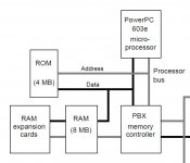
Here's your Duo 2300c Block Diagram, it's exactly what's on your Blackbird PPC Upgrade target as I understand it.

2300c-FSB-Block_Diagram.JPG

2300c

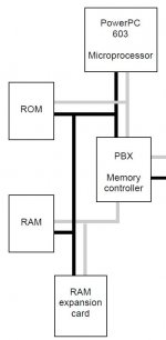
The block diagrams of 2300c and 1400 are all but indistinguishable.

1400-FSB-Block_Diagram.JPG

1400

edit: at this level (FSB?) the 2300c and 1400 are identical but for the CPU board interconnect.*** The Delta DevNote for the Enhanced 1400 (166MHz/Cache) doesn't provide a block diagram update for the CPU card unless it's on one of the pages that appear to be blank.

*** Different Max RAM provisions are mere details related to intentional hobbling of the 2300c/PPC upgrade path that Apple had promised, but never really wanted to ship for the Duo System. With IDE AND SCSI buses on board for HDD, Color AND Grayscale connectors for LCDs on board makes the 2300c the Swiss Army Knife of the PPC menagerie. Plans were to hang T-REX/PCMCIA Card Cage of the 1400 off the Duo's Docking Connector. That's why there is so much vacant cubic underneath the PCB in the UltraDock series. Getting that setup running has been a sporadic journey of fifteen years.

 
Last edited by a moderator:

Paralel

Well-known member
Those are exactly the type of heat sinks I was considering. Looks like he FX's heat dissipation could be manageable.

750FX seems the obvious choice for my 1400 project, 20x gets it to 666MHz with 512k  of on die cache vs. my Crescendo PB at 466MHz with 1MB on the backside.

Here's your Duo 2300c Block Diagram, it's exactly what's on your Blackbird PPC Upgrade target as I understand it.

edit: at this level (FSB?) the 2300c and 1400 are identical but for the CPU board interconnect.*** The Delta DevNote for the Enhanced 1400 (166MHz/Cache) doesn't provide a block diagram update for the CPU card unless it's on one of the pages that appear to be blank.

*** Different Max RAM provisions are mere details related to intentional hobbling of the 2300c/PPC upgrade path that Apple had promised, but never really wanted to ship for the Duo System. With IDE AND SCSI buses on board for HDD, Color AND Grayscale connectors for LCDs on board makes the 2300c the Swiss Army Knife of the PPC menagerie. Plans were to hang T-REX/PCMCIA Card Cage of the 1400 off the Duo's Docking Connector. That's why there is so much vacant cubic underneath the PCB in the UltraDock series. Getting that setup running has been a sporadic journey of fifteen years.


I had no idea the 2300 was so similar in architecture. I can completely see what you are talking about. It appears that our two projects do certainly intersect. Anything you learn can be applied to future plans for the BlackBird project, and vice-versa.

 
Last edited by a moderator:
Those are exactly the type of heat sinks I was considering. Looks like he FX's heat dissipation would be reasonable.
750FX/GX are the fastest coolest per clock of all G3 due to its process it uses ~4w at 800MHz

also they have software controlled clocking there are 2 PLL's those cards you see in that pic the white chip 1 holds a 750FX@800mhz and that heatsink can keep it stable at 1GHz same the TSI107 is a 7410 which can hit 600+ with that sink

we wrote a program to control the clocks within AmigaOS 3.X

 
Last edited by a moderator:

Paralel

Well-known member
750FX/GX are the fastest coolest per clock of all G3 due to its process it uses ~4w at 800MHz

also they have software controlled clocking there are 2 PLL's


4W, that's it? That would be 50% of the maximum that the 740 puts out. Very nice.

Software controlled clocking? Hmm. I'd have to read up about that and how Mac's work with those.

 
4W, that's it? That would be 50% of the maximum that the 740 puts out. Very nice.

Software controlled clocking? Hmm. I'd have to read up about that and how Mac's work with those.
it will stay at default hardwired speed till set by software or powersaving states

 
Last edited by a moderator:

Trash80toHP_Mini

NIGHT STALKER
From my read the FX uses a standard PLL setup with the option of software control. Later versions jettisoned standard PLL clock multipliers. Haven't looked at the GX since I found an unlimited supply of the FX.

 
Top