• Updated 2023-07-12: Hello, Guest! Welcome back, and be sure to check out this follow-up post about our outage a week or so ago.

Need help hunting the other end of a trace on a SE/30

lowlytech

Well-known member
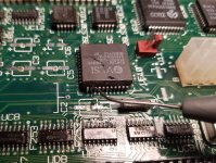
Got my first SE/30 this week and have been looking over the traces after getting the battery and caps off the board.  I have a questionable pin on UE10 that I believe is pin 10.  The schematic shows this line connecting to something off screen.  Can someone help me find a test point to check for continuity from this pin in the picture?  Also have a question on the same schematic file  (SE30_P7.GIF).  I appear to have two broke lines on UC12 Pin 1 and 2 going to RP2 pin 18/17.  This schematic shows a break in those lines.  Is this a mistake on the schematic as I don't get continuity from these two test points, but I do get continuity from RP2 18/17 to R42 and R43 on the back of the board.  
se30.jpg

 
Last edited by a moderator:

Bolle

Well-known member
You are pointing at pin 41 in that picture.

You start counting counter clockwise at the small dot on top of the package a few pins to the right of the one you are pointing at.


lowlytech

Well-known member
Thanks Bolle for that info, I wasn't quite sure if I was counting in the right direction. This is really my first time tracking down pins on IC's that isn't in a DIP package.  I checked pin 41 on the schematic and it looks like it is in the same group as pin 10.  It labels pin 41 as A0.  Looks like it goes to (1-6) A (0.31).  What point is this on the board so I can make sure I have a good connection?  I visually tried to follow the trace but it looks like it ducks underneath the Y2 oscillator crystal.

 
Last edited by a moderator:

tattar8

Well-known member
That's the address bus.  That notation means that the address bus also occurs on pages 1-6, and is 32 bits wide.  The line you're looking for is A0, the least significant bit.  From a quick look through the pages of the schematic, it connects to the 68030, as well as to UK6 pin 10 and UD8 pin 4.


lowlytech

Well-known member
Thanks Tattar8 for explaining what the numbers/markings referred to.  When I get home I will have another look at the schematics to try to follow that logic and make the connection on how to read and understand the schematic fully between pages.  Appreciate the time and help with this.  Hopefully I don't find too many more questionable connections.  Will keep everyone posted on the progress.  Hopefully we can get this SE/30 back up and running.


macclassic

Well-known member
Is there a guide somewhere on how to read and understand Apple schematics between pages? as I have traces to follow too and would like to know how to do this.


lowlytech

Well-known member
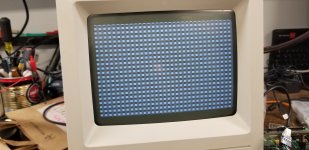
Got the board recapped and looks like I still have broken traces somewhere.   I get the startup chime but otherwise it;s WYSIWYG..

20190430_213857.jpg


lowlytech

Well-known member
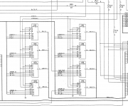
Awesome, Thanks Bolle for the heads up on where to look.  One question which will probably echo macclassic's question.  In this section of the schematics it looks like the Ux8 chips are listed twice.  I assume this is just for each side of pins?  Also say UA8 for example.  Pin 5 just goes to nothing and says VADR (7).  Where would I try to find the other end of this connection?

Untitled.png


lowlytech

Well-known member
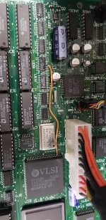
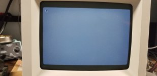
The culprit was UD8, pin 4 to the Glue chip, pin 77.  Everything else seems fine, as this was the only wire I had to run an now it comes up normal looking.  I even got the original 40MB Quantum drive un gooed and it appears to be working without issue for the moment.  Thanks again for all the direction and help with this.  I appreciate it. 

20190505_183801.jpg

20190505_183649.jpg


Bolle

Well-known member
That’s address bit 0.

For those mux chips they just list each of the two 4->1 muxes as seperate unit in the schematics, that’s why they appear twice.

 
Top