@macintosh2002 I'd strongly suggest looking into ChipQuik low melting point alloy. I've ordered one of these kits and if it works the way I've seen it work in videos online then it should make chip removal much easier. Basically the solder is an alloy of Iridium which is quite expensive hence the kits only include a small amount of it. But you only need a small amount to remove each chip and it effectively reduces the melting point of the solder to a much lower level which the chip can tolerate more or less indefinitely.
-
Updated 2023-07-12: Hello, Guest! Welcome back, and be sure to check out this follow-up post about our outage a week or so ago.
You are using an out of date browser. It may not display this or other websites correctly.
You should upgrade or use an alternative browser.
You should upgrade or use an alternative browser.
Macintosh SE/30 logicboard recreation (thread revival)
- Thread starter Bolle
- Start date
macintosh2002
Well-known member
That’s sounds great, in their data sheet I found „Rework - Removes QFP's, PLCC's, SOIC's, and chip components under 300 degrees Fahrenheit... 150C“. It’s definitely worth a try, thanks@macintosh2002 I'd strongly suggest looking into ChipQuik low melting point alloy. I've ordered one of these kits and if it works the way I've seen it work in videos online then it should make chip removal much easier. Basically the solder is an alloy of Iridium which is quite expensive hence the kits only include a small amount of it. But you only need a small amount to remove each chip and it effectively reduces the melting point of the solder to a much lower level which the chip can tolerate more or less indefinitely.
robin-fo
Well-known member
Did you try to repair the board first? The damage appears to be in a very limited area compared to other battery victims I have seen.@craig1410
Thank you very much for sharing your experience!
I got a SE/30 with a leaking Maxwell battery from 11/90 which destroyed the logicboard and will place an order at JLCPCB with a green presoldered (backside) board to rebuild my SE/30.
I already started with desoldering some chips, but that's way harder than I thought it would be, especially when it comes to the soldered cpu and PLCC chips.
edit:
I'm not sure, but did you use a socket for the cpu instead of direct soldering the CPU to the board? If so, which one did you use please?
You can buy the '030 socket here: https://www.exxoshost.co.uk/atari/store2/
I have a spare board in case you don‘t want to order five from JLC…
macintosh2002
Well-known member
You’re right - but no, I did not try to repair it, because there are lots of pads and traces eaten away from the battery juice at the RAM MUX chips. I will order five, you’ll never know when you need another board, and there are a lot of SE/30 macs with damaged PCB. Especially now when @Bolle gave us the possibility to built a new PCB.Did you try to repair the board first? The damage appears to be in a very limited area compared to other battery victims I have seen.
You can buy the '030 socket here: https://www.exxoshost.co.uk/atari/store2/
I have a spare board in case you don‘t want to order five from JLC…
Thank you for that link, I‘m not sure if it is in joshc BOM.
Last edited:
superjer2000
Well-known member
@macintosh2002 or others: If it’s more economic to order multiple boards (with the passives on the back prepopulated) I’d be interested in putting my name down for 2.
I’m ok to prepay for the boards and then would pay for shipping when they come back.
If it doesn’t bring the price down might not make sense.
I’m ok to prepay for the boards and then would pay for shipping when they come back.
If it doesn’t bring the price down might not make sense.
superjer2000
Well-known member
Scratch that... I didn't realize how inexpensive JLPCB is... I ordered 5 boards with the SMT service, although a few components were unavailable (with one of those being the most populous unfortunately but I figured supplies might get worse) for around $200 shipped. That's crazy. I did the better finishes.@macintosh2002 or others: If it’s more economic to order multiple boards (with the passives on the back prepopulated) I’d be interested in putting my name down for 2.
I’m ok to prepay for the boards and then would pay for shipping when they come back.
If it doesn’t bring the price down might not make sense.
The first board will be be used to move components over from my first battery bomb SE/30. On first inspection I thought the board would be OK but unfortunately there are a number of vias (well 4 at least) that are gone and for the cost of the boards vs. the cost of time troubleshooting, I ordered the boards.
Of course, this doesn't factor in the cost of Bolle's time. Thank you for making these available!!
Good to see a few more folks embarking on this journey - it's way more fun than diagnosing broken traces and vias and soldering in bodge wires I can tell you that much! 
Some tips I would give on sequence of populating components as follows. Others please chip in if you have better/alternate advice. This is just what worked for me. Note that I was using a 10x electronics assembly microscope which I'd say was invaluable but perhaps you could manage with younger eyes and/or a decent bench magnifier.
Firstly, populate the backside first if not done during PCB manufacture. At this stage the topside is completely flat and will sit nice and stable on your workbench. I'd recommend an anti-static soft rubber mat but keep it clean to avoid any debris scratching the solder mask.
From here on the general principle is start low and work up, away from the PCB, and prefer SMD components which require sideways access for soldering (ie. PLCC chips) over other devices which can be soldered easily from directly above. Just keep thinking, if I install "this" component, which other components does that make difficult to access?
On the backside I did all the resistors first, starting from the lowest resistance and working up through each value. I think that's quicker than finding R1 then looking up to see what value it is then getting that component out and fitting it before going on to R2. There is a certain pattern to the numbering sequence on the silkscreen with a few exceptions so it's quite easy to do one resistance value at a time. It also minimises the chance of getting component values mixed up which is especially important with capacitors since they often aren't marked up the same as resistors.
After that I repeated the process with capacitors but only on the backside for now. I then harvested and fitted the SMD inductors from my donor board, taking care to keep track of which is which by sticking them to a piece of tape marked with L8, L9.... L22. I didn't fit the through hole L1 or L2 at this stage. Lastly I fitted the SMD diodes D4-D19.
On the topside I started with the PLCC chips but you could also have started with the likes of the small SMD semiconductors like D1, D2, Q1, Q2, Q3, F1, F2, F3 etc. If harvesting the PLCC chips from a donor, take care to remove them with minimum heat and take ESD static precautions. Also, clean them thoroughly and remove any old solder from the pins and make sure all the pins are nice and straight and the chip sits flat without rocking on a raised pin. I found a little soft fibre pencil was good for cleaning the pins along with IPA.
When fitting the PLCC chips, alignment is really important so take time to get it right before soldering the first pin. Use a good gel flux and good quality solder wire. You might choose to solder pin by pin like me or drag solder but that's up to you. If doing it pin by pin then try to use a very fine tip so that you can heat the PAD first and then feed in the solder such that it bridges to the pin naturally. If you heat the pin first or simultaneously the solder will tend to stick to the pin and you won't be able to get it to drop down to the pad. If you do catch the pin first and have this problem then just use wick to remove the excess solder, apply more flux and try again. I tended to solder bottom right pin first, then a diagonally opposite pin then recheck alignment before running round the whole chip.
After the PLCCs I did the various SOIC chips and resistor packs and all other SMD components including tantalum caps before turning attention to the through hole components. Again I tried to tackle the lower components first such as IC sockets (turned pin style) before the crystals, axial caps, S1, S2, L1, L2, RP1, RP2, RP3. The last things to go in were J5, J8, J12, battery holder and the SIMM sockets. I'm waiting on the serial, ADB and DB-25 and DB-19 connectors arriving as well as the PDC socket so will fit these soon. I also need to harvest the metal rear support bracket from the donor board and will fit that too.
Lastly, try to clean flux off components as you go rather than waiting until the end. I don't mean do this for every SMD resistor, you can do those every 10 mins or so of assembly, but for other, larger components it's easier to clean them sooner rather than wait until later. It also provides a good opportunity to inspect the soldering and do any rework before moving on and potentially obstructing the rework with other components.
That's all for now other than to say to treat this as a marathon not a sprint and walk away regularly to eat, exercise, sleep and spend time with family. It's very unlikely you'll finish this in one day so pace yourself and avoid silly mistakes. I started mine on Jan 1st and got it booting on Jan 6th albeit some of that time was waiting on parts. I didn't keep track of time spent but it must have been upwards of 15 hours although a lot of that (~60%) was harvesting donor parts and cleaning them up.
Enjoy!
robin-fo
Well-known member
My specimen is slowly nearing completion after an initial 12 hours shift today. I decided to use PLCC sockets to be able to easily transfer the chips to a second board which I am planning to populate, without having to desolder them a second time.
Attachments
Looking good!
I was very tempted to use PLCC sockets as well but didn't think it would be very easy to solder around the plastic base of the socket. Looks like you managed it though. Did you have to trim away some of the plastic or did it just naturally melt back a bit due to the soldering iron proximity?
I prefer your black resistor packs to the yellow ones I got.")
Good luck with the rest of the build - looking forward to hearing about your first boot up!
I was very tempted to use PLCC sockets as well but didn't think it would be very easy to solder around the plastic base of the socket. Looks like you managed it though. Did you have to trim away some of the plastic or did it just naturally melt back a bit due to the soldering iron proximity?
I prefer your black resistor packs to the yellow ones I got.
Good luck with the rest of the build - looking forward to hearing about your first boot up!
robin-fo
Well-known member
Thanks a lot @craig1410! I didn‘t have to trim the plastic and maybe it wouldn‘t even be necessary. The wavy lines around the holes in the bottom come from the soldering iron touching the plastic. Space is indeed very limited down there and I probably wouln‘t have been able to solder every leg without scorching the plastic.
The next big job will be the desoldering of all PLCC chips on the donor board (which still looks very intact as I almost entirely used new parts until now). I am also still waiting for the SIMMs and the CPU socket to arrive from England and the spare CPU, the 68882 and a 68000 (for another project) to arrive from China.
The next big job will be the desoldering of all PLCC chips on the donor board (which still looks very intact as I almost entirely used new parts until now). I am also still waiting for the SIMMs and the CPU socket to arrive from England and the spare CPU, the 68882 and a 68000 (for another project) to arrive from China.
Daniël
Well-known member
Thanks a lot @craig1410! I didn‘t have to trim the plastic and maybe it wouldn‘t even be necessary. The wavy lines around the holes in the bottom come from the soldering iron touching the plastic. Space is indeed very limited down there and I probably wouln‘t have been able to solder every leg without scorching the plastic.
Is there a specific reason you kept the plastic? As far as I know, it's meant to be removed if it's going to be hand soldered.
I recently saw this video on YouTube where they just cut the entire floor out of the socket. It certainly makes it much easier to solder but presumably the socket floor is there to provide mechanical integrity so I worry this might not be a great solution. I prefer the way @robin-fo did it by working around the floor as much as possible, provided of course that the solder joints themselves are good enough.
Garrett B
Well-known member
Probably a dumb question but where are you finding your sockets/ports/headers? Are you using peconnectors.com? I am starting a build here soon but still need to do some ordering. I agree that although it might be more work up front, adding a socket would save lots of time in the event of a bad chip!My specimen is slowly nearing completion after an initial 12 hours shift today. I decided to use PLCC sockets to be able to easily transfer the chips to a second board which I am planning to populate, without having to desolder them a second time.
Scott Squires
Well-known member
I was putting together an order from peconnectors the other day. After having 15 different items in my cart, it told me that was the max number of line items allowed. If I wanted to order more, I would have to make it a separate order. And pay a fresh additional $16 shipping. Really now?
robin-fo
Well-known member
I got most parts from mouser (very recommendable!). Of course you won‘t find any SIMM sockets, DB19 ports or ’030 sockets there. Peconnectors might be an interesting supplier as long as you are in the US, but they appear to have no interest in shipping to the rest of the world.Probably a dumb question but where are you finding your sockets/ports/headers? Are you using peconnectors.com? I am starting a build here soon but still need to do some ordering. I agree that although it might be more work up front, adding a socket would save lots of time in the event of a bad chip!
If I can get my SE/30 to work, I will publish my mouser chart to make it easier for others.
I also got most parts from mouser using the links in the SE/30 BOM referenced elsewhere in this thread. I created a "Project" in mouser for this but it looks like I can only share a project using an email address. However, I created a "Basket" instead and have shared it via this link:
Mouser Basket for SE/30
Hopefully I'm not breaking any forum rules by sharing this link since it's only for forum member convenience and there is no financial gain for me.
Note that one item is currently backordered so I'd suggest looking for an equivalent. In general, anyone using this link in future will need to look out for any backordered items and find an alternative. Some backorder times can be very long on Mouser. Also, note that this basket includes the passive components for the backside so don't order these if you're using the JLCPCB pick and place service.
Other suppliers I used are as suggested on the SE/30 BOM document for the UK. ie. RS Components, exxoshost.co.uk, silicon-ark.co.uk
HTH
superjer2000
Well-known member
@cig1410 Your posts are super helpful on this. Thanks!. I do keep hoping to see a TL;DR at the bottom of one of them that says just send you the board and parts and you’ll send back a working se/30 logic board….
Are you guys ordering new connectors instead of harvesting for that shiny new board feeling or were the donor board parts rust from a battery bomb or other? I had intended to harvest but I might just order the mouser cart (other than the pre soldered passives)
Are you guys ordering new connectors instead of harvesting for that shiny new board feeling or were the donor board parts rust from a battery bomb or other? I had intended to harvest but I might just order the mouser cart (other than the pre soldered passives)
@superjer2000 haha, I’d be quite happy to stop my day job and refurbish SE/30 boards instead but I suspect it might be a bad business decision! These things are a labour of love I think, rather than a career prospect! 
Re using new connectors, in my case the PDC socket was quite badly corroded by the battery bomb so a new one certainly was a necessity. But also, and more generally for other connectors which have soldered mechanical support tabs like the ADB, SCSI, Floppy and Serial connectors, it’s just a hassle to harvest them without causing damage to them in the process. I removed the 25 pin D connector for the external SCSI from my donor board but it was a real struggle to both remove the solder AND get the mechanical fixing posts to disengage. In retrospect probably the way to do it is to just cut most of the PCB away from the connector with a dremel or similar tool and then remove the PCB fragments with hot air or desoldering wick etc.
But even if you succeed, best case you end up with a 30+ year old connector with contact oxidation, mechanical wear and tear and cosmetic defects which seems a shame on what is otherwise largely a “new” board. Now, if you’re on a tight budget or trying to make a profit from this endeavour then you might make different choices because these connectors are not cheap. I’m fortunate this is more of a hobby.
I should also mention that, although I ordered the connector parts from mouser according to the SE/30 BOM spreadsheet, I have not yet received them so can’t confirm personally that the parts in my mouser basket are 100% correct. This includes the PDC, ADB, Serial and 25 pin D sockets. I’m hoping they might arrive today as they were last seen departing France this morning on their way from the US to UK. I’ll post an update once I have them and have confirmed they are the right parts. I’m pretty confident they will be though. All other parts in my mouser basket have already been fitted to my board so all good there.
Good luck with your refurb!
ironborn65
Well-known member
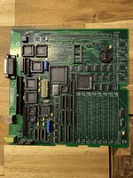
Where do you get those brand new 4MB SIMM modules?I recently finished testing on the final (so far) working revision of the SE/30 board.
Below is my initial post from before the site crash on how everything started:
All things on the "left to do" list had been worked out before the site crash.
Just recently I found the time to finally order a batch of revision 2 boards with the SCSI blooper fixed and PLCC32 ROM sockets added.
Now just look at this beauty:
View attachment 35973
Passed all tests, no bodge wires needed and already has been running 3 days straight now without any hiccups.
Board files, reverse engineered PAL files and BOM available on github:

GitHub - TheRealBolle/SE30: Macintosh SE/30 logicboard recreation
Macintosh SE/30 logicboard recreation. Contribute to TheRealBolle/SE30 development by creating an account on GitHub.github.com
Many thanks go to...
@joshc for putting together the BOM
@cheesestraws for supporting me with reverse engineering the PALs
@Siliconinsider for making those beautiful die shots of the GLUE https://www.siliconpr0n.org/archive/doku.php?id=bercovici:apple:344s0602-a - who's going to give recreating that one a go now?
@Kai Robinson for putting together pick and place files (also found in the github)
and finally @GeekDot for bugging me into starting with this project in the first place and working on the (not yet working) in system ROM flashing software when using the PLCC32 ROM sockets (more on that later - probably)
I'll clean up the github over the next days and add some more descriptive information.
thanks
Similar threads
- Replies
- 99
- Views
- 11K
- Replies
- 16
- Views
- 682