You are using an out of date browser. It may not display this or other websites correctly.
You should upgrade or use an alternative browser.
You should upgrade or use an alternative browser.
2.5" SCSI SSD Project
- Thread starter techknight
- Start date
Lookin' Gooooood!!!!!!!! :approve:
Don't be afraid to use INTENTIONALLY placed "rework" wire thru-holes to simplify things on a two layer board!
I finally put a Digital Caliper on the 3.5" Drive .1" O.C. Header Pins. At approx .025" square for the pins, there appears to be approx. .08" available in between the pins to run your traces (less one pad width & insulation spaces) in between pins.
Is the board maker using a thickness just a hair less than .08" for your ProtoBoard? :?:
Actually, a .025" (25 mils) square pin has ~.036" diagonal. Plating a through hole reduces it's diameter a bit, so you would use a 39 to 46 mil hole for that pin.I finally put a Digital Caliper on the 3.5" Drive .1" O.C. Header Pins. At approx .025" square for the pins, there appears to be approx. .08" available in between the pins to run your traces (less one pad width & insulation spaces) in between pins.
Is the board maker using a thickness just a hair less than .08" for your ProtoBoard? :?:
Then putting an 8 mil annulus (ring) around the hole gives you a total pad diameter of 56 - 62 mils. Call it 60 mils. So your pad edge to pad edge distance will be about .040" (40 mils) in practice.
If you're using a service with 6 mil traces & spacing, you can get two traces between those holes though. Space - trace - space - trace - space. Yields 5 X .006" = 30 mils. Or use 8 mils and the distance is exactly 40 mils.
Still, that extra 10 mils in the .006" example (40 - 30 mils) can be added to the spaces next to the holes. Space(11 mils) - trace (6 mils) - space (6 mils) - trace (6 mils) - space (11 mils). Total 40 mils.
It's no fun trying to solder pins in place when there's a trace just six mils away from the pad. If your board has solder mask with a margin less than 6 mils, it's not really a problem though until you have to rework something and some of the solder mask gets removed.
Well, hopefully i will keep everything away from those pins, except traces. i doubt ill have to rework the SCSI header anyway.
Thanks for the corrections, it was very late and I wasn't seeing straight . . . (=@#&^%&*?<%^ . . . time change!  )
)
im a "just learning" CAD Noob. so that went through one ear and out the other. hehe. Ive been used to ExpressPCB when it was just point and click. add it in. its just proprietary, and VERY expensive production run, which is why i moved off of it.
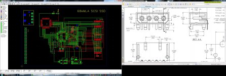
Anyone have the standard ol' 50-pin IDC right angle header datasheet kicking around anywhere? i need the dimensions so i can punch this stuff up in cad.
trag's math isnt working out for me. but again, im a noob so i could be doing it all wrong.
trag's math isnt working out for me. but again, im a noob so i could be doing it all wrong.
Well . . . I understand the SCSI connector Pads and the Molex Connector Pads . . .
. . . the rest is Greek to me! :I
I've never done any SMT design. The only experience w/Gerber Files I've ever had was cutting Silk Screen Stencils and the final RubyLith Film Positives of the three cards and solder mask art that we sent to a local PCB house on one of Gerber's Sign Making Machines (Mine had the 30" Plotter, most were 15") driven by the MacSignMaker Card & Software circa '89 - '90!
Yer' makin' me feel really old, kiddo! )
)
But it's lookin' GOOD! AFAIK, Trag was just saying that you'll have no trouble at all routing a single trace in between the inside pads of the SCSI connector to reach the outboard row of pads and that, if needed (at this scale) you can run two traces between the header pads, but assembly/debugging might not be much fun if you did so.
Keep up the good work, comrade! :approve:
. . . the rest is Greek to me! :I
I've never done any SMT design. The only experience w/Gerber Files I've ever had was cutting Silk Screen Stencils and the final RubyLith Film Positives of the three cards and solder mask art that we sent to a local PCB house on one of Gerber's Sign Making Machines (Mine had the 30" Plotter, most were 15") driven by the MacSignMaker Card & Software circa '89 - '90!
Yer' makin' me feel really old, kiddo!
But it's lookin' GOOD! AFAIK, Trag was just saying that you'll have no trouble at all routing a single trace in between the inside pads of the SCSI connector to reach the outboard row of pads and that, if needed (at this scale) you can run two traces between the header pads, but assembly/debugging might not be much fun if you did so.
Keep up the good work, comrade! :approve:
Yea, im still a pup. 1985. lol.
1985! :O That makes you the same age as my son! :lol:
:lol: 
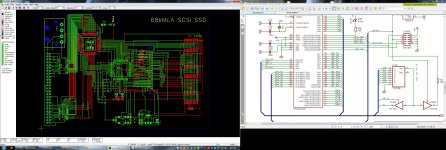
Anyway, way to go kiddo! You only needed two tween-pad traces after all, it's pretty cool that the outboard pads are for the alternate ground lines on the ribbon cable, eh?
[ ] ]'>
] ]'>
Anyway, way to go kiddo! You only needed two tween-pad traces after all, it's pretty cool that the outboard pads are for the alternate ground lines on the ribbon cable, eh?
[
That looks great, T!
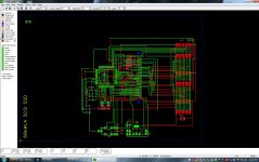
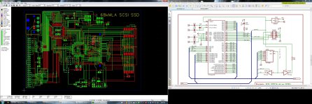
The only possibility I see for problems would be the overlapping of the bus lines from layer to layer from that QFP (?) to the two cable driver ICs (?) creating a bit of crosstalk between bus lines on each layer a/o between the two buses through the FRP. Dunno if I've read it right though, but throwing alternating ground lines between the signal traces on both sides and offsetting the two buses so that the opposite numbers are ground lines from layer to layer might not be a bad idea, if you have the room w/o reshuffling everything about to achieve it.
Take that with a grain of salt, it's late again and my brain shut down around noon today . . . :-/
I dont have the room. or i would have done something like that.
I just sent the board off to have fabbed. setup fees and all, it ran about 72 dollars. OUCH.
But hey, its a prototype, and its cheaper than what i would have paid for a double-board, 4 layer sandwhich.
I just sent the board off to have fabbed. setup fees and all, it ran about 72 dollars. OUCH.
But hey, its a prototype, and its cheaper than what i would have paid for a double-board, 4 layer sandwhich.
Congratulations, you've got your proof of concept prototype/debugging design out the door and off to the Fab Lab in a form factor that's more workable for assembly, for testing and still in a salable package!I just sent the board off to have fabbed. setup fees and all, it ran about 72 dollars. OUCH.
But hey, its a prototype, and its cheaper than what i would have paid for a double-board, 4 layer sandwhich.
EXCELLENT work, kiddo! :approve:
What's the turn around time and expected assembly completion? :?:
Double that and use a correction factor of three for the software coding/debugging estimate!
Depends on when the fab house sends off the panel.
I am using SparkFun's service, which is the cheapest for single board runs. Because they put a bunch of submitted designs on a single panel for fab, its cheaper per person this way.
So i gotta wait for the panel to fill, which doesnt take long, and then get sent off. 3 weeks max, 1 week min.
Also i got the parts i didnt have on hand, ordered tonight. Another $50 bucks there.
The transceivers are 26 bucks a peice from digikey 8-o
So i went straight over to TI and got 2 samples. heck with 26 a piece until i know if its gonna work.
So, regardless, if this works out, i am gonna have to sell it off just to fund the 2.5" project, which was my ultimate goal. I only have limited funds available for this hobby stuff, and i damn near ran out. lol.
Also i ordered enough parts to build 10 of them. so a total of $50 in parts, approx 10 bucks a board.
this is MINUS the transceivers, and AVRs/Crystals, as i have that stuff kicking around.
I did end up making a couple of errors on the board, but hey, i can fix that though. no routing errors, just forgetting "resistors" errors. one on the RESET signals, and another one on the LOF signal to the CF slot.
That sounds a lot like the early days of VSLI, boards (ICs) were ganged up into one panel (die) and run the same way this service is doing it now.
My dad had all the VLSI Texts Laying around the house along with Fortran, Cobol and a bunch of other programming Texts, a hunk of CORE Memory, PunchCards and "Think" plaques.
I loved the VLSI Texts . . . as art books! :
Keep us posted, I'm sure a limited run of your corrected Prototype will fund the next step . . .
. . . and allow you to hold onto your first prototype!
Ya. im worried about speeds as well. Using 16mhz clock source for 2 8-bit micros are bottlenecks.
however, its expected to get roughly 1.5 to 3mbps, or 150 to 300KBytes/s depending on the compact flash used, etc...
and this also varies HEAVILY on the cross-talk. lol.
Worse comes to worse, i can use that conductive "pen" silver oxide, and coat the entire set of traces with it. and draw it over to a ground via.
As far as CORE memory, that stuff is unique how it works. I still cant quite understand how it works. I restored a broken down seeburg jukebox that used the CORE memory as its TORMAT selection device. same concept.
Similar threads
- Replies
- 26
- Views
- 1K
- Replies
- 19
- Views
- 1K


