-
Updated 2023-07-12: Hello, Guest! Welcome back, and be sure to check out this follow-up post about our outage a week or so ago.
You are using an out of date browser. It may not display this or other websites correctly.
You should upgrade or use an alternative browser.
You should upgrade or use an alternative browser.
Soldering new vram onto Quadra 630 motherboard?
- Thread starter LaPorta
- Start date
Trash80toHP_Mini
NIGHT STALKER
Look up the ICs, I'm pretty sure those are 128x4 DRAM ICs making up the 4MB of built-in system memory? My Q630 board is MIA ATM, so I can't check. What's the pincount/package type of that memory? Sounds like 4MB of soldered memory in Bank A in the Q605/LC475 from your description, which fits in with the 630's heritage.
The 6290 appears to use a pair higher density ICs (DRAM?) for its of 1MB VRAM. This pittance was standard from 630 through 6400 and was finally increased to a barely adequate (my opinion) 2MB in the 6500/TAM.
Dunno about piggybacking same/same ICs, but it would be interesting to see if addressing VRAM doubled in that manner might be a possibility?
Last edited by a moderator:
it's a worthy experiment. There's a good chance that the Valkyrie video controller won't address more than 1MB of VRAM, or that the address lines are not present, but who knows. The Hardware developer note (http://mirror.informatimago.com/next/developer.apple.com/documentation/Hardware/Developer_Notes/Macintosh_CPUs-68K_Desktop/Mac_LC_630_Quadra_630.pdf) pg. 16, says that the Valkyrie is similar to the display portion of the MEMCjr in the Q605 (1MB limit) and the DAFB in the Q700 and Q900 (2 MB?). The note also says that the video memory is plain old RAM, not any special dual ported RAM or such.
Late edit: and the note says there's 8MB of address space allocated to VRAM. Doesn't mean much, but at least it's not limited to 1MB. Figure 2-2, pg. 19.
One megabyte of memory, thirty-two bits wide, in 8 chips is made of 8 1Mbit chips which are each 4 bits wide. So, 256K X 4 chips, X 8. If you want to double that, then you need to find 512K X 4 chips. The pinout will be standard. 256K means that there are 18 address bits, and at least 9 address pins on each chip (addresses are multiplexed, sent 1/2 at a time). If there are only 9 address pins, then it can't be done, absent discovering an unused DRAM address pin on the Valkyrie chip. 512K X n memory chips require at least 10 address pins.
However, there is a tiny bit of hope, as the 256K chips could be addressed in an 8 X 10 or 10 X 8 pattern instead of 9 X 9, in which case 10 address pins would be present.
As someone else wrote, the first step should be to identify the VRAM chips and find a datasheet for them.
Oh, one last thing, memory capacities of chips seemed to always increase by factors of 4, so 512K X 4 chips may not exist. You may have to go to 1M X 4. That can still work with 10 address pins though, so if there are 10 the first hurdle is cleared.
It looks like I have a bunch of Oki MSM514400D 1M X 4 chips on hand, somewhere in the attic. These are also what the super common 4MB 32 pin SIMM would have usually have built out of, so you can salvage them from those too.
Looking at the datasheet for the M2M514400, the chip has 20 pins in a 26 pin pattern. I.e. There are two rows of pins with room for 13 pins, but the middle 3 pins in each row are omitted.
View attachment MSM514400E.pdf
Last edited by a moderator:
Trash80toHP_Mini
NIGHT STALKER
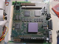
LaPorta, any chance of taking some hi res pics of you logic board? Can't find mine and it's beginning to piss me off. It can't drive me crazy, but it could bring on an episode. :blink:
Trash80toHP_Mini
NIGHT STALKER
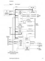
Hrmmm . . . does "DMA8-0" designations in the Q630 and PM5260 Block Diagrams differ from "A8-0" I've seen elsewhere?
Q630
PM5260
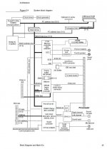
I'm wondering if the three bank setup of Video Memory could be problematic as it's tightly intertwined with the video input module's workings?
Doesn't sound anywhere near as simple as adding a second VRAM SIMM to a 605 if you find DMA9.
Q630

PM5260

I'm wondering if the three bank setup of Video Memory could be problematic as it's tightly intertwined with the video input module's workings?
Display RAM
The display memory in the Macintosh LC 630 and Macintosh Quadra 630 computers
is separate from the main memory. To reduce the cost of the computer, the display
memory is implemented with DRAM devices instead of more expensive VRAM devices.
The display memory consists of 1 MB of 60 ns DRAM devices configured to make a 32-bit
data bus. The display memory cannot be expanded.
The display memory contains three separate frame buffers. The first frame buffer holds
the graphics data—the display that is generated by the computer. The other two frame
buffers hold video data from the video input module. The video data frame buffers are
used alternately: while one is supplying data to be sent to the video monitor, the other is
receiving the next frame of video input.
The display data generated by the computer can have pixel depths of 1, 2, 4, 8, or 16 bits
for monitors up to 640 by 480 pixels and 1, 2, 4, or 8 for larger monitors and the
800-by-600-pixel display on the multiscan monitor. Data from the video input module
is always stored and transferred at 16 bits per pixel. The video frame buffers support
live video in a 320-by-240-pixel frame at 30 frames per second.
Doesn't sound anywhere near as simple as adding a second VRAM SIMM to a 605 if you find DMA9.
Last edited by a moderator:
Trash80toHP_Mini
NIGHT STALKER
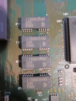
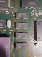
Took another look at the 5260 DevNote and 6290 board. It has a quartet of TMS418160DZ-70 DRAM ICs that look ripe for stacking if the 10th bit be found. Might be an easier package/board combo for the stuffing the Valkyrie, a bit of Wagner that. [} ]
]
http://willem.engen.nl/projects/bc2000-dev/TMS418160.pdf
http://willem.engen.nl/projects/bc2000-dev/TMS418160.pdf
Trash80toHP_Mini
NIGHT STALKER
Strange, I can't find the datasheet or spec on that DRAM IC. Seems strange that the 6290 would have a quartet of lower capacity chips than the 630? Is there another pair on the "solder side" of the board.
Trash80toHP_Mini
NIGHT STALKER
It must be the 32bit/64bit bus width bump in that case.
edit: gotta come up with the datasheet for whatcha got there already to check the pinouts, if there's no room for that tenth bit, it's stacking, not replacement.
Given the tight integration of "video data frame buffers" in Valkyrie, I'm not even bettin' a nickel of finding that tenth bit. My bet would have to be on not being able to find A9 even on the second gen Valkyrie-AR on the Alchemy boards. :/
Last edited by a moderator:
Franklinstein
Well-known member
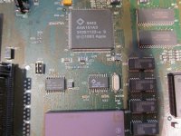
The Valkyrie (and later Valkyrie-AR) were originally produced by Sierra Semiconductor, long a producer of RAMDAC/CLUT chips (Apple used them for years across many models) but not well-known for other video-related chips. The only integrated graphics chip they produced was the Falcon64, which saw very little use and was fairly quickly discontinued; Sierra exited the video market altogether in 1995ish (later Valkyrie chips are stamped with AT&T logos, so maybe Ma Bell picked up that division).
It's possible that the Valkyrie is a relative of the Falcon64 designed to interface directly to the 68040 bus, and the Valkyrie-AR the same except built to sit directly on the 60x bus, rather than the Falcon64's ISA and/or PCI bus interface.
VGAMuseum has a STB Horizon 64 that shows one of the only implementations of the Falcon64, complete with two soldered RAM chips and sockets for two more. It appears that this chip addresses memory in two banks of two 512k chips. Whether the Valkyrie was actually related to the Falcon64 or not, I can't say, but if it is, it appears that more memory would require additional chips, not replacing the existing chips with higher-capacity ones.
Unfortunately, there does not seem to be any documentation available from either Apple or Sierra/PMC-Sierra/Microsemi/AT&T/Lucent/whoever-owns-it-now regarding these legacy devices, so it's not easy to figure out how these chips address memory. Maybe stacking would be possible? Otherwise I have no idea.
Because these are DRAMs, they interleave the addresses. So adding one address line would add two address bits to the address space.
So, if a tenth address bit is available, one could address 1M X 16 (these are 256K X 16) chips. Finding 16 bit wide memory chips is not easy.
Alternatively, as someone mentioned above, there might be additional bank signals -- extra RAS lines perhaps that are not used on Valkyrie.
@Trash80toHP_Mini the memory chips soldered on the 6400 are also 16 bits wide (but four of them to get 64 bit bus on PPC). I think they pads are htere but the memory is omitted on the 6500. Might be able to get part numbers for higher capacity chips by looking at those.
Attachments
Similar threads
- Replies
- 9
- Views
- 355
- Replies
- 61
- Views
- 6K

