Done, and removed the blockquote from around the content of the edited second post.
Mods are gods
")
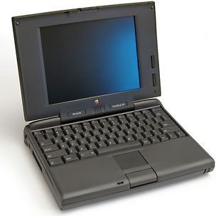
I finally got around to disassembling the 520. Recently got my IC extractor and I wanted to try it out anyways. Suffice to say, it did not disappoint.

I'm going to say this is a draw. It appears there are three rows of pins. The first inner two, closest to the connector dock, seem to be through-hole/thruhole. The outer row, furthest from the connector, look to be surface-mounted.

From the other side of the board, we can see the inner two rows breach through the board.

I captured the battery connector SMC, which is north of the PDA port, and is also thru-hole. Note the similarities.

Angled view to see the posts/pins

Overhead view; it's hard to see all three rows of pins here. Someone is going to have a lot of fun unsoldering that! I will say, it will probably not be me. But..yeah

Finally, I tried to capture all three rows from an angle. Note, behind the surface-mounted outer row

Maybe a reflow would be best to remove this PDA connector? Then, I suppose you could furnish a breakout board, or pin converter, that would connect to a new adapter of your choice. That's just my $0.02