Good to know - now the other question I'd have is if 60mhz tripled from 20mhz performs better than 50mhz doubled from 25mhz for graphically intensive applications (think Marathon), where (AFAIK) you get a benefit from the faster vampire video. That, or using an FPGA to build out a 68030 that can handle the 70mhz clock and sticking that in the accelerator (not sure if that's doable, though)
You are using an out of date browser. It may not display this or other websites correctly.
You should upgrade or use an alternative browser.
You should upgrade or use an alternative browser.
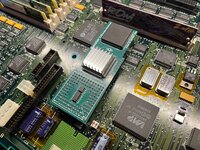
Interware Booster 30-SE50F Info Dump
- Thread starter zigzagjoe
- Start date
zigzagjoe
Well-known member
I had the same thought. I think 25mhz x2 to 50mhz would definitely be more well-rounded and also would have increased video bandwidth. However It would be a complete rewrite of the logic to work at 2x, I tinkered with it a little but didn't finish the job and have no plans to do so. I don't have much interest in the IIsi, nor has there been much interest in IIsi cards so I don't plan to make any new cards that specifically target IIsi.Good to know - now the other question I'd have is if 60mhz tripled from 20mhz performs better than 50mhz doubled from 25mhz for graphically intensive applications (think Marathon), where (AFAIK) you get a benefit from the faster vampire video. That, or using an FPGA to build out a 68030 that can handle the 70mhz clock and sticking that in the accelerator (not sure if that's doable, though)
Unfortunately there are no complete 68030 softcores, so FPGA is out. By the time you've gone through all the effort to interface the FPGA though you'd not necessarily beholden to a strict multiplier. Not something I have any interest in playing with anyways.
Zarwox
Member
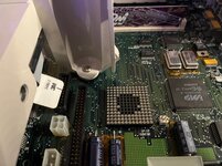
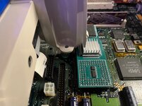
Wow! I just got the Socket Booster 2.0 and for giggles I tried it out in my IIcx. It works great!
Before and after comparison using Speedometer 3.23

Unfortunately there is a clearance issue with the drive cage so it won't stay in this machine but it was a fun test, and meditative solder work")

Thanks for creating this! If you ever decide to recreate a fully IIcx compatible PCB layout for this design, sign me up!
Before and after comparison using Speedometer 3.23
Unfortunately there is a clearance issue with the drive cage so it won't stay in this machine but it was a fun test, and meditative solder work
Thanks for creating this! If you ever decide to recreate a fully IIcx compatible PCB layout for this design, sign me up!
Attachments
zigzagjoe
Well-known member
Wow! I just got the Socket Booster 2.0 and for giggles I tried it out in my IIcx. It works great!
Before and after comparison using Speedometer 3.23
View attachment 82657
Unfortunately there is a clearance issue with the drive cage so it won't stay in this machine but it was a fun test, and meditative solder work
View attachment 82662
Thanks for creating this! If you ever decide to recreate a fully IIcx compatible PCB layout for this design, sign me up!
Glad to see you got the socket installed OK and it's all working. Sorry about the clearance problem... I don't have an entire IIcx chassis to work with - just a logic board - so I didn't even think about that as apple's cases are quite roomy inside.
It's not quite clear from the picture - is it just the heatsink making contact with the drive cage?
Zarwox
Member
I agree with you. I was also very surprised and did not notice the issue until the very very end of assembly.
The heatsink is indeed the first object making contact with the cage but even if removed it will hit the PCB. In theory one may get away with cutting material off the cylindrical support "column" of the drive cage. I'm hesitant to recommend it though since the cage, with this one important screw point, along with the PSU is what provides rigidity to the case. Especially when standing upright and the column itself is what takes the load when a something heavy, like a monitor, is placed on top in desktop mode. Without the internal support of the drive cage and PSU the case cracks easily (I learned that the hard way many years ago). Sure you usually have a lightweight LCD monitor nowadays but the plastics in these cases are brittle now (and people like us tends to stack them)
The heatsink is indeed the first object making contact with the cage but even if removed it will hit the PCB. In theory one may get away with cutting material off the cylindrical support "column" of the drive cage. I'm hesitant to recommend it though since the cage, with this one important screw point, along with the PSU is what provides rigidity to the case. Especially when standing upright and the column itself is what takes the load when a something heavy, like a monitor, is placed on top in desktop mode. Without the internal support of the drive cage and PSU the case cracks easily (I learned that the hard way many years ago). Sure you usually have a lightweight LCD monitor nowadays but the plastics in these cases are brittle now (and people like us tends to stack them)
Attachments
Last edited:
zigzagjoe
Well-known member
Gah. Yeah, that's a non-starter. I wouldn't recommend hacking on the original mount either. If I ever find a case for my IIcx LB I'll see about designing a 3D printed replacement.
As you said, it'd otherwise have to be a completely different board for it to clear, and at the moment I don't have plans to make one. IIcx seems to be an uncommon machine, I got my board as a new-old-stock service part.
Yeah, that's a non-starter. I wouldn't recommend hacking on the original mount either. If I ever find a case for my IIcx LB I'll see about designing a 3D printed replacement. As you said, it'd otherwise have to be a completely different board for it to clear, and at the moment I don't have plans to make one. IIcx seems to be an uncommon machine, I got my board as a new-old-stock service part.
Zarwox
Member
It's a fairly big 3D print but definitely doable and will fit on most printer beds I believe. I also thought of creating an intermediate board for moving the CPU socket a bit towards the back of the LB but I'm a little worried about the clearance under the PSU.
Here is a thread with a photo of the Daystar IIcx adapter showing the cut-out they had to do to get around the mount.
https://68kmla.org/bb/index.php?threads/found-iicx-with-daystar-cpu-adapter.36024/
Here is a thread with a photo of the Daystar IIcx adapter showing the cut-out they had to do to get around the mount.
https://68kmla.org/bb/index.php?threads/found-iicx-with-daystar-cpu-adapter.36024/
Daniël
Well-known member
Would some sort of interposer PCB work?
I imagine a PCB with pins to insert to the logic board socket, with a PGA socket on the right of those, 1:1 connected, to move the accelerator further away from the drive cage.
Not sure what the impact on signal integrity and such would be, nor how sturdy that solution would be, but I imagine something like this should be possible.
It might be an easier way to fix it than designing and printing an entirely different drive cage.
zigzagjoe
Well-known member
Yep! The developer note does not mention the IIsi specific signals added to the connector. Wonderful, isn't it?The IIsi Developer Note shows pin B2 as ground in the diagram on Page 64 and pin list on page 67.
Is there another conflicting doc?
Here's the relevant DC&D excerpt.

(continued discussion from trading post thread regarding booster IIsi and cache cards)
Fizzbinn
Well-known member
Yep! The developer note does not mention the IIsi specific signals added to the connector. Wonderful, isn't it?
Here's the relevant DC&D excerpt.
View attachment 83028
(continued discussion from trading post thread regarding booster IIsi and cache cards)
I thought there might be something like this! Wonderful indeed... Curious, perhaps dumb question, what is this "DC&D" doc?
I think I will try your suggestion of removing the B2 pin from your IIsi Booster and testing again with the 3 Cache cards I have. I have to admit it's giving me an icky feeling to remove a pin like that though!
zigzagjoe
Well-known member
It's definitely a bit barbaric, but easiest way forward. To do it properly, the connectors would have to be removed, B2 on the PCB in both locations carefully and cleanly drilled so as to not short ground and power planes, then connector reinstalled and a jumper ran between the pins. Just about as ugly, and a lot more work.I thought there might be something like this! Wonderful indeed... Curious, perhaps dumb question, what is this "DC&D" doc?
I think I will try your suggestion of removing the B2 pin from your IIsi Booster and testing again with the 3 Cache cards I have. I have to admit it's giving me an icky feeling to remove a pin like that though!
DC&D is designing cards and drivers, it gives detailed info on the various expansion interfaces as well as some sample implementations.
Attachments
Fizzbinn
Well-known member
It's definitely a bit barbaric, but easiest way forward. To do it properly, the connectors would have to be removed, B2 on the PCB in both locations carefully and cleanly drilled so as to not short ground and power planes, then connector reinstalled and a jumper ran between the pins. Just about as ugly, and a lot more work.
DC&D is designing cards and drivers, it gives detailed info on the various expansion interfaces as well as some sample implementations.
Thanks for the doc, super interesting. It looks like Apple is saying the "real & supported " PDS 68030 Direct Slot expansion interface for the IIsi, as documented in the IIsi Dev note, is the one on their official PDS "Direct Slot adapter card", they are basically saying the logic board connector is different. Seems like a lot of vendors didn't tow that line, e.g. Ethernet cards for the IIsi that I've seen all look to be designed to connect to the logic board directly.
zigzagjoe
Well-known member
Well, not all experiments are successful but here's a quick write up on my latest one. This feature probably won't make it to prime time, but it was an interesting experiment.
It started with the thought - Modern ROM SIMMs have a drastically faster response time of ~70ns as compared to the original ROM's ~150ns. In theory, if I modify the booster logic it would be possible to 'shortcut' ROM access in order to increase ROM read performance by 2x or more.
First a couple of findings about the GLUE:
So instead I modified my Booster code to issue an internal bus cycle termination after ~ 70ns, which is a good deal faster than the 230ns the complete cycle normally takes. Less than a third of the time, so we should have a lot more ROM bandwidth!
Results?
Speedometer reported no performance change. Boo.
System info indicated 2% faster quickdraw performance, mostly in the few algorithmically heavy tests (ie. drawing shapes)
Macbench reported 10% faster quickdraw performance. (It mostly uses algorithmically heavy tests rather than memory-constrained stuff like CopyBits)
Individual macbench subtests ranged from a minimum of 2% faster to a maximum of 41% (frame round rect) with most being 10-30%.
Interestingly, macbench shows the stock CPU to be slightly faster at "copybits - copy" by 15%. I'll have to validate that...
A little underwhelming. I suppose it makes sense QuickDraw would be the code in ROM that would be accessed most heavily. But, most code is going to be running out of RAM so it would not benefit from this unless it hit a ROM routine with a hotspot (CPU intensive portion) just a bit too big to fit in the 68030 internal caches. And RAM access is as slow as ever, so fundamental performance elsewhere won't change.... unless an L2 cache was in play, anyways.
Admittedly, these benchmarks aren't really heavilly accessing the toolbox anyways outside of QuickDraw tests. ROM shadowing isn't a new idea, and supposedly it helps Quadras a bit; perhaps the IIsi ROM is largely bypassed by the newer System 7.5 I was testing with. Open to ideas if anyone knows a benchmark that'd really hammer toolbox calls.
It started with the thought - Modern ROM SIMMs have a drastically faster response time of ~70ns as compared to the original ROM's ~150ns. In theory, if I modify the booster logic it would be possible to 'shortcut' ROM access in order to increase ROM read performance by 2x or more.
First a couple of findings about the GLUE:
- ROMOE signal on GLUE does *not* use /AS or /DS as a qualifier. So, at any times the ROM may be activated if the upper address lines A31-A28 encode $4 for the ROM space, including between bus cycles. Eeek.
- DSACK0/1 driven in response to /AS + address $40000000 is run by a state machine inside GLUE, it does not cancel earlier if /AS goes away early.
So instead I modified my Booster code to issue an internal bus cycle termination after ~ 70ns, which is a good deal faster than the 230ns the complete cycle normally takes. Less than a third of the time, so we should have a lot more ROM bandwidth!
Results?
Speedometer reported no performance change. Boo.
System info indicated 2% faster quickdraw performance, mostly in the few algorithmically heavy tests (ie. drawing shapes)
Macbench reported 10% faster quickdraw performance. (It mostly uses algorithmically heavy tests rather than memory-constrained stuff like CopyBits)
Individual macbench subtests ranged from a minimum of 2% faster to a maximum of 41% (frame round rect) with most being 10-30%.
Interestingly, macbench shows the stock CPU to be slightly faster at "copybits - copy" by 15%. I'll have to validate that...
A little underwhelming. I suppose it makes sense QuickDraw would be the code in ROM that would be accessed most heavily. But, most code is going to be running out of RAM so it would not benefit from this unless it hit a ROM routine with a hotspot (CPU intensive portion) just a bit too big to fit in the 68030 internal caches. And RAM access is as slow as ever, so fundamental performance elsewhere won't change.... unless an L2 cache was in play, anyways.
Admittedly, these benchmarks aren't really heavilly accessing the toolbox anyways outside of QuickDraw tests. ROM shadowing isn't a new idea, and supposedly it helps Quadras a bit; perhaps the IIsi ROM is largely bypassed by the newer System 7.5 I was testing with. Open to ideas if anyone knows a benchmark that'd really hammer toolbox calls.
Last edited:
David Cook
Well-known member
Admittedly, these benchmarks aren't really heavilly accessing the toolbox anyways outside
I have always wanted to record a heatmap (profile) of where a Mac spends most of its time. I figure something could just monitor the bus address and increment a counter for each (or perhaps a block at a time). I don't know how it would account for time spent in the CPU cache.
I recognize my understanding of bus usage is naive. And, I assume Apple or third-parties already did this type of work at some point to determine bottlenecks. Still, conceptually, it might provide a lead for optimization.
eharmon
Well-known member
Does the ROM code have a built in wait loop for ROM access? The Quadras do to try to time ROM access to the respective bus speed. It's one of the things you can overclock with a custom ROM by removing wait states.A little underwhelming. I suppose it makes sense QuickDraw would be the code in ROM that would be accessed most heavily. But, most code is going to be running out of RAM so it would not benefit from this unless it hit a ROM routine with a hotspot (CPU intensive portion) just a bit too big to fit in the 68030 internal caches. And RAM access is as slow as ever, so fundamental performance elsewhere won't change.... unless an L2 cache was in play, anyways.
Admittedly, these benchmarks aren't really heavilly accessing the toolbox anyways outside of QuickDraw tests. ROM shadowing isn't a new idea, and supposedly it helps Quadras a bit; perhaps the IIsi ROM is largely bypassed by the newer System 7.5 I was testing with. Open to ideas if anyone knows a benchmark that'd really hammer toolbox calls.
7.5 definitely patches a significant amount of the ROM code for older devices, so I would expect a IIsi ROM to be largely supplanted by patches.
An interesting benchmark might be boot time. There's heavy toolbox access in general and the patches aren't loaded for a bit meaning it's going to be hammering the ROM. Especially boot from a RAM disk to remove SCSI latency.
zigzagjoe
Well-known member
I have always wanted to record a heatmap (profile) of where a Mac spends most of its time. I figure something could just monitor the bus address and increment a counter for each (or perhaps a block at a time). I don't know how it would account for time spent in the CPU cache.
I recognize my understanding of bus usage is naive. And, I assume Apple or third-parties already did this type of work at some point to determine bottlenecks. Still, conceptually, it might provide a lead for optimization.
Yes, that is essentially how my 68030 ICE (in circuit emulator) works. It does disable cache (by default) since that prevents the external hardware in the ICE device from having full visibility into the code execution as you pointed out. Maybe I need to break it out and try to profile the ROM with it, I was planning to try to profile my CF driver with it.
Does the ROM code have a built in wait loop for ROM access? The Quadras do to try to time ROM access to the respective bus speed. It's one of the things you can overclock with a custom ROM by removing wait states.
7.5 definitely patches a significant amount of the ROM code for older devices, so I would expect a IIsi ROM to be largely supplanted by patches.
An interesting benchmark might be boot time. There's heavy toolbox access in general and the patches aren't loaded for a bit meaning it's going to be hammering the ROM. Especially boot from a RAM disk to remove SCSI latency.
No, not quite the same here. Those wait states govern the timing put into the programmable hardware in the Quadras, so that behavior is all mutable. In the SE/30 the waitstates on ROM that are all hardcoded by the GLUE, but happily, due to the behavior noted earlier since ROMOE is not qualified with /AS, there's no actual need to pass /AS_LOCAL (47mhz domain) to /AS_PDS (system 15.667mhz domain) in order to trigger the GLUE ROM acknowledge cycle since the ROM is going to output data anyways.
Instead, I wait a few cycles in my CPLD's logic then assert the appropriate bus termination to the fast CPU. This reduces the ROM access cycle down from about 256 ns to 105 ns. Or, about 16 MB/s of bandwidth to the ROM becomes 38MB/s (!). Could be interesting to do a read benchmark to confirm this / ROMdisk testing.
I measured boot time with 7.5 just now. About a 2 second delta - so definitely a change. Using my compactflash instead of SCSI to boot from, this saw about another second of reduction. It's something. I may break it out to a jumper. Any booster 2.0 cards could be upgraded to have this function as though it'd require my soldering a wire to a test point to act in place of a physical switch/jumper that'd be missing. Or some other bodge.
For the RAMdisk boot, I assume you're talking with a rominator or similar where you can hold a key to make it boot from a copy of the ROMdisk in RAM?
Here's a screenshot(s) of the delta as measured by macbench.

Last edited:
zigzagjoe
Well-known member
Of course, 38MB/s theoretical is all great but you do still need to *do* something with the read data I wrote a quick benchmark to read ROM as fast as possible to determine (in some sense) what the benefit works out to be. Since we're not running the code out of RAM, this isn't precisely the same thing, but it gives a sense of one of the possible scenarios such as when a ROMdisk is used.
Ran this at boot at BootRec time (just before happy mac) to reduce stealing CPU time from me. At some point, I'll run it bare metal with no mac ROM to get a sense of what difference that might make.
Stock: 940 ticks
Booster2: 661 (~ 11 seconds)
Booster2 + ROM-Booster: 399 (~ 40% faster)
Also, as expected, this technique does not work on the IIsi: presumably, it does qualify ROMOE with /AS, unlike the more primitive logic in the SE/30.
I wrote a quick benchmark to read ROM as fast as possible to determine (in some sense) what the benefit works out to be. Since we're not running the code out of RAM, this isn't precisely the same thing, but it gives a sense of one of the possible scenarios such as when a ROMdisk is used.Ran this at boot at BootRec time (just before happy mac) to reduce stealing CPU time from me. At some point, I'll run it bare metal with no mac ROM to get a sense of what difference that might make.
Stock: 940 ticks
Booster2: 661 (~ 11 seconds)
Booster2 + ROM-Booster: 399 (~ 40% faster)
C:
static void ROMbenchmark () {
    volatile uint32_t *LM_ticks = ((volatile uint32_t*)0x16A); /*[GLOBAL VAR] Current number of ticks since system startup (long), ~ 60 /second */
    Ptr ROM = (Ptr)0x40800000; // 32/24 safe ROM start

    dbg_prints("ROM Benchmark start\n");

    uint32_t end, start = *LM_ticks;

    asm volatile (  // this needs to be small and fit in instruction cache
        "move.l #128, %%d1      " "\n" // 1MB * 128
        "2:                     " "\n"
        "move.l %0,%%a1         " "\n" // load address into a1
        "move.l #0x3FFF, %%d0   " "\n" // 16384 = 1MB, size of 24 bit ROM space
        "1:                     " "\n"
        ".rept  16              " "\n" // 16 repetitions
        "move.l (%%a1)+,%%d2    " "\n" // 4 byte read from *%a1, postincrement to avoid data cache
        ".endr                  " "\n"
        "dbra   %%d0, 1b        " "\n" // inner loop
        "dbra   %%d1, 2b        " "\n" // outer loop
    :
    :"a" (ROM)
    :"d0","d1","d2","a1"
    );

    end = *LM_ticks;
    dbg_labeldec("ROM Benchmark elapsed time",end - start);
    while(1); // hang here
}
Also, as expected, this technique does not work on the IIsi: presumably, it does qualify ROMOE with /AS, unlike the more primitive logic in the SE/30.
David Cook
Well-known member
postincrement to avoid data cache
Can you explain this comment about avoiding the data cache?
zigzagjoe
Well-known member
Can you explain this comment about avoiding the data cache?
If I hit the same address over and over, it'll just end up in the 256 byte data cache (if it is enabled), so the cache will return that value rather than causing a bus cycle. So in this case, stock CPU without the increment ends up taking ~570 ticks instead since it's not actually reading from ROM other than the time to fill the cache line.
Similar threads
- Replies
- 8
- Views
- 1K
- Replies
- 58
- Views
- 10K
- Replies
- 13
- Views
- 2K
- Replies
- 23
- Views
- 2K
- Replies
- 171
- Views
- 25K