Interware Booster 30-SE50F Info Dump

treellama

Well-known member
Design validation has completed and I've added support for the IIsi ROMs to its logic. Some further changes were required to enable using a newer clock generator as there are alignment requirements for the phase shift/modified duty cycle clocks. @treellama is going to find out with one of my prototypes if it works in the IIx/IIcx too - I'm thinking this will be a yes.

It totally works in the IIx!

interware_comparison.png
 

halkyardo

Well-known member
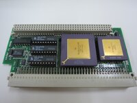
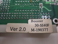
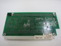
I was lucky enough to get my hands on one of zigzagjoe's prototype boards and have a couple of notes to share.

My main interest in getting my hands on one was to validate my ethernet card with it - on that front, I'm happy to say that it works really well, and the faster processor does wonders for network throughput, confirming my suspicion that networking performance on the SE/30 is largely CPU-bound, rather than IO bound.

However, the same can't be said for my RasterOps ColorBoard 264. With the accelerator installed, it never displays its splash screen, and the system locks up hard at the point in the boot process where the driver would normally load. We chased this down to an *extremely* lazy DSACK rise time - so slow that it was causing the bus cycle *after* an access to terminate prematurely because it was still at a logic-low voltage well into the next cycle, with often disastrous counsequences.

The channels in the attached scope trace are:
  1. Board select (/AS & addr=0xFBxxxxxx)
  2. /DSACK0
  3. /DSACK1
  4. /AS
You can see how the second access to the board terminates immediately while /DSACK1 meanders its way back up - but then an access to some other address has nice sharp /DSACKx edges.

It's still a bit of a mystery as to why the rise time is so slow on that card specifically - adding extra pullup resistors to /DSACK made things a little bit better but didn't fix it entirely. I was able to get it mostly working by adding some external logic to explicitly drive /DSACK0 and 1 high during the period between /AS getting deasserted and the next cycle starting. With this brute force 'fix' in place, the card mostly works, but occasionally has display glitches as though some writes aren't quite making it through. I suspect that it's just not quite up to the tighter timing requirements imposed by the faster processor.

1708643701561.jpeg
C'mon DSACK, you're letting the side down!

1708643901640.jpeg
Success! (sort of)
 
Last edited:

zigzagjoe

Well-known member
Great writeup. This is the exact same symptom I experience with an old Shiva Etherport SE30 card - unfortunately I don't have quite as much visibility into the signal quality, but I'm suspecting it's a similar issue where a signal gets held too long and rolls into the next 47mhz clock cycle. Hopefully I can tweak on the GAL logic when I have a new testbed card in hand to try to get some better behavior.
 

halkyardo

Well-known member
Spoke a little bit too soon about getting the ColorBoard working - the rise time issues are only half of the story, it also appears to be holding DSACK asserted for too long as well. Most of the time, my fast rise-time hack was enough to make it work, but in some cases, the ColorBoard was still holding DSACK down for long enough to interfere with subsequent cycles. Most of the time this would just cause graphics corruption, but it will occasionally just crash the machine outright.

There are a few other options to explore, still - tweaking the GAL logic on the accelerator is probably the most promising way to resolve this, we're working on some ideas there.
 

Melkhior

Well-known member
It's still a bit of a mystery as to why the rise time is so slow on that card specifically
Cost-cutting / didn't read the CPU manual properly (I'm betting the first!)

Quoting from the '030 UM on asynchronous bus cycles:
The device must remove its data and negate DSACKx within approximately one clock period
That's negate, not tri-state or deassert. The device should actively drive the signal to logic 0 (so +5V) before tri-stating for the next bus cycle, as relying on pull-ups only might be too slow. IIRC I have a design document somewhere explaining this more thoroughly than Motorola's documentation (or is it for the '040? same idea). I suspect your card doesn't do it and for a sufficiently slow clock, sufficiently strong pull-up, and sufficiently low capacitance, DSACKx are negated in time so it all works. Change something, and things go seriously haywire...
 

zigzagjoe

Well-known member
Cost-cutting / didn't read the CPU manual properly (I'm betting the first!)

Quoting from the '030 UM on asynchronous bus cycles:

That's negate, not tri-state or deassert. The device should actively drive the signal to logic 0 (so +5V) before tri-stating for the next bus cycle, as relying on pull-ups only might be too slow. IIRC I have a design document somewhere explaining this more thoroughly than Motorola's documentation (or is it for the '040? same idea). I suspect your card doesn't do it and for a sufficiently slow clock, sufficiently strong pull-up, and sufficiently low capacitance, DSACKx are negated in time so it all works. Change something, and things go seriously haywire...

Huh. I didn't realize about the negate part. I've got a project underway that I hadn't immediately planned for that on, so that may get interesting...
 

Melkhior

Well-known member
Huh. I didn't realize about the negate part. I've got a project underway that I hadn't immediately planned for that on, so that may get interesting...
The documentation doesn't make it obvious in any one place, other sources are sometimes clearer. The important bit is a note right at the beginning of the UM in the preface:
In this manual, assertion and negation are used to specify forcing a
signal
to a particular state. In particular, assertion and assert refer
to a signal that is active or true; negation and negate indicate a
signal that is inactive or false. These terms are used independently
of the voltage level (high or low) that they represent.
(emphasis mine).

In the flowchart the negation of /DSACKx (or, in my case, /STERM) is also explicit, as it is in the text, but the exact meaning it not repeated and the subsequent tri-stating (which is also indispensable!) is not there either, hence the potential ambiguity.

IIRC, both SBus and NuBus (which are both IEEE standard, this might explain that) are much clearer on the subject and so I was forewarned when doing the IIsIFPGA and QuadraFPGA.
 

halkyardo

Well-known member
That's negate, not tri-state or deassert. The device should actively drive the signal to logic 0 (so +5V) before tri-stating for the next bus cycle, as relying on pull-ups only might be too slow. IIRC I have a design document somewhere explaining this more thoroughly than Motorola's documentation (or is it for the '040? same idea). I suspect your card doesn't do it and for a sufficiently slow clock, sufficiently strong pull-up, and sufficiently low capacitance, DSACKx are negated in time so it all works. Change something, and things go seriously haywire...

Huh! That would make sense, I suppose.

I took a closer look at the rise time on my own card, and it's also pretty marginal. In my case it was easy enough to add a 'fixup' state to drive DSACK high between being deselected and /AS next going low. Very glad I switched to a CPLD for my glue logic!
 

zigzagjoe

Well-known member
Updated card compatibility list:

Known good:
Interware GrandVimage
Asante MacCon
Farallon TP594
@halkyardo SEthernet :)
Carrera 040 (Yes: You can switch between the ~50mhz 68030 and the 68040! Isn't that a hoot?)

Known incompatible:
Shiva Etherport 30
Rasterops Colorboard 264
Micron Xceed (All models)
 

Jockelill

Well-known member
Question, can the original Interware booster be reflashed to also support the IIsi ROM? Or the ROM modified?
 

zigzagjoe

Well-known member
Question, can the original Interware booster be reflashed to also support the IIsi ROM? Or the ROM modified?

Yep, it's straightforward enough to add the sensitive addresses to the existing logic so as to support IIsi ROM also - just requires a bit of ROM spelunking :)
 

zigzagjoe

Well-known member
So, an interesting find. On the original card, there was a pin that was wired to /STERM.LOCAL but always cut, and while the GAL has /STERM.PDS wired and a few others, the equations in that GAL don't reference them - effectively unused.

After thinking on this the answer became clear: if this is the current revision, why are they still cutting traces and has unused ones wired? Because it can be used in a situation where it is needed. The 30-50F board doesn't work in the IIsi, certainly lack of /STERM is at least part of the problem, also trying to run 60mhz could be a problem. But as the multiplier frequency is controlled by feedback from the GALs, for a hypothetical IIsi design you can just double instead, which probably leaves enough free logic to do the /STERM stuff not possible on the SE30 board.

Only picture I found of the 30-SI40F IIsi design confirms it.... it's an identical board, just 3 different GALs. Not immediately useful information, but interesting nonetheless :)

1723817359143.jpeg
 

Jockelill

Well-known member
Interesting! When I first got this card I had to try it in my IIsi and I can confirm it does not work, but physically it does fit, so this makes perfect sense! Now the real question is if you can recreate those GALS 😅😅

Btw, where did you find that picture?
 

zigzagjoe

Well-known member
Interesting! When I first got this card I had to try it in my IIsi and I can confirm it does not work, but physically it does fit, so this makes perfect sense! Now the real question is if you can recreate those GALS 😅😅

Btw, where did you find that picture?
I found it in an old yahoo auctions listing. Not any great detail or pictures, but it's something. https://aucview.aucfan.com/yahoo/k194200581/

I'm working on a new CPLD-based booster design, as I've been spoiled by the CPLD i'm using on my 30Video boards. I'm primarily doing it so I can stop programming SOIC ATF chips, but the CPLD has quite a bit more capacity to work with. I'm going to build in the possibility to both implement /STERM on the SE/30 version, as well as extra signals that would seem to be needed for an IIsi version. So, perhaps? I suspect it's probably a bit simpler logic since it's a power of 2.

I also had a thought that it'd be nice to directly slow access to the sound/video/serial hardware rather than the roundabout method used now (slow the code accessing the hardware), and I think that would be very doable.
 

Attachments

  • k194200581.2.jpg
    k194200581.2.jpg
    162.8 KB · Views: 15
  • k194200581.3.jpg
    k194200581.3.jpg
    174.6 KB · Views: 11
  • k194200581.1.jpg
    k194200581.1.jpg
    179 KB · Views: 10
Top