David Cook
Well-known member
The following is an obnoxiously long technical explanation of why the Macintosh Classic II, LC, LC II, and Performa equivalents have a 10MB RAM limit. For most of this post, I use the Classic II as an example.
TLDR:
1. Not enough address pins connected between CPU and memory controller.
2. Not enough address pins connected between memory controller and onboard RAM / SIMM slots.
2. Standard ROM routine given a table that doesn't search above 10MB, thus ROM routine never thinks there is more than 10MB.
16-BIT DATA BUS
The Classic II (LC, LC II, etc) has a 32-bit processor. Apple implemented a 16-bit RAM data bus on these particular computers. This means that if the processor wants to operate on a full 32-bits of newly read information from RAM, it needs two reads (2 reads x 16 bits=32 bits). If the RAM data bus was 32 bits, like on the Mac IIci, then the processor would only need a single read (1 read x 32 bits=32 bits). So, worst case, it takes twice as long to read that piece of information on a Classic II.
Caveats:
1. The processor has built-in variables (registers) and 256 bytes of built-in memory (cache) for both instructions and data (except 68020). This retains recently read information at the full 32-bits.
2. The ROM is directly connected to the full 32-bit address bus. Therefore, reads of system ROM routines are full speed.
See below that "RAM data bus (16)" is 16-bit, but ROM is "D31-0" which is 32-bits.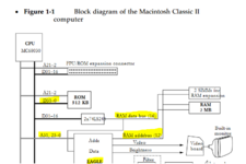
Therefore, just because new RAM reads take two accesses (16-bit data bus), the computer is not actually running twice as slow all the time. Significant portions of the time are in full 32-bit portions of the architecture.
The size of the data bus only affects speed. It has no impact on the total amount of memory accessible. For example, it doesn't limit total memory to 16 MB or 10 MB or anything like that.
ADDRESS BUS
Address bus is much more complicated.
In the figure above, 25-bits (A31 + A0-A23) of addressing is going into the Eagle Chip. That means 2^25=33,554,432/(1024*1204)=32MB of memory can theoretically be addressed between the CPU and Eagle.
The Eagle claims only 12 bits going to the RAM. What? That's only 2^12=4096 bytes of memory. No, that isn't what is appears to be.
DRAM is like a bathroom tile floor or a piece of graph paper. It has rows and columns. Each time a memory chip is accessed, it is given a row address and then a column address to finally look up the data. For example, "please look up the data at row 5 column 2". To save on pins, the same pins are used for both the row and column address, but at different times. Another two pins signal the times when to look up the row address (RAS) and when to look up the column address (CAS). For example, address_pins=5, RAS, address_pins=2, CAS, is like me saying "Look up 5th row" (you move your finger to that row) and then I say "2nd column" (you move your finger across the row until you find column 2 and then tell me what you see).
So, in the diagram above, the Eagle chip can lookup 2^12=4096 different rows followed by 2^12=4096 different columns. That's 4096*4096=16,777,216 different total memory cells. 16 million!
Looking at the Bomarc schematic, we see that onboard DRAM is only given 10 address lines (RA0 to RA9). That's 2^10 * 2^10 = 1,048,576 only 1 million cell locations. Fortunately, there are 4 memory chips (U13, U14, U17, U19) being accessed in parallel, so that's 4,194,304 million cell locations. But, oh no, each memory chip can only output half a byte (4-bits, 1 nibble), so that's 4,194,304 million cells / 2 cells per byte = 2,097,152 = 2 MB of RAM. That's exactly what the Classic II has onboard.
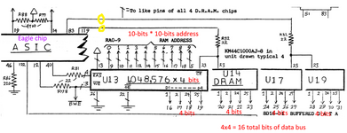
Fortunately, on the LC II, they use 8 memory chips (U12-U19) to have 4 MB of RAM. They added two more column select pins to access the additional memory.
If you wanted 4 MB of onboard RAM on the Classic II, you could cut pins 83 and 119 (see above) and feed them into a daughter board that would connect them to the original set of chips when RA10 (the next highest address bit) was low and connect them to a new set of four chips when RA10 was high. Of course, you'll also need to feed all the added chip pins (address, data, power, R/W, etc) from the existing onboard memory to the new daughterboard memory. That's a lot of cutting and soldering.
Let's try looking elsewhere.
SIMM Slots
Standard 30-pin SIMMs have 12 address lines (RA0-RA11) and 8 data lines (not counting parity which is unused on this Mac). Remember, these are DRAM address lines not CPU address lines. So, that's 2^12 * 2^12 = 16,777,216 worth of 8-bit data cells. 16 MB! Fantastic? Sadly, no. The Eagle chip does not connect to SIMM socket pin 24 (RA11). So, that's only 2^11 * 2^11 = 4,194,304. 4 MB! Oh, that's exactly the maximum memory SIMM that the Classic II accepts per slot. That's 8 MB total for the pair.

Why Do You Have to Install a Matching Pair of SIMMs?
The Eagle chip addresses both SIMM slots at the same time, using 8 bits from one slot and 8 bits from the other slot to fill its 16-bit data bus. That's why both slots need to be filled and they both need to be the same size SIMMs. If one SIMM was missing, half the bits would be missing on each read. If one SIMM was larger, the smaller SIMM would either repeat bits from earlier in memory (wrong bits) or again be missing half the bits.
Let's say you cram the next biggest size of SIMMs into those slots. 8 MB 30-pin SIMMs don't exist. It goes 4MB->16 MB. Now you've got a pair of 16 MB SIMMs for a total of 32 MB of memory. Because the Eagle chip only has 11 of 12 address pins connected, each 16 MB SIMM will be seen as 4 MB with the extra never being accessed because those higher row/column addresses are never hit. You're back to having a pair of 4 MB SIMMs (8 MB total) as far as the Eagle chip is concerned.
The Classic II schematic is missing descriptions for pins 89 and 103 of the Eagle chip. I haven't checked all the pins, so some pins might not be listed at all. There is a possibility that an undocumented pin on the Eagle chip is the desired missing 12th address pin (RA11). Cutting whatever trace (likely ground?) connects to SIMM socket pin 24 and hooking it up to the undocumented RA11 Eagle chip pin would then theoretically support 16 MB SIMMs.
Even in the unlikely event that Eagle has an undocumented RA11 pin out, it would also need to be designed to service this additional memory during refresh cycles. Let's assume it does that.
Ok, so now you have 2MB on onboard RAM and 32 MB of SIMM RAM. But, the Eagle chip is only given 24 CPU address bits = 16 MB. The CPU doesn't have any way to address most of the memory. Best case, you'll now have 16 MB maximum instead of 10 MB.
ROM MEMORY MAPPING
Assuming you've overcome hardware limitations and somehow hooked up some extra RAM. Mapping it to the OS is another obstacle. In the ROM, there is a startup routine called SizeMemory in the SizeMem.a source file. In this code, the Eagle chip is referred to as the VISA. This chip family is also used in the LC and LC II.
Onboard memory is physically mapped using the three highest bits in VsExp(RBVAddr). These registers directly correlate to the Eagle chip hardware, so it isn't like you can just modify the ROM to add more bits.
Cool aside: Switching to 560x384 graphics mode (such as used by the Apple IIe card) is controlled by the lowest bit in this register.
The memory configuration registers tell the Macintosh the starting address of the onboard RAM. Surprisingly, the SIMMs are mapped below the onboard RAM in memory. Before hitting the standard sizing code, a subroutine called VisaSplit carefully moves onboard memory above any possible installed SIMM RAM. If you have 2MB of onboard RAM, it moves it to the Addr8MB boundary. If you have 4 MB of onboard RAM, it moves it to either the Addr4MB boundary or the Addr8MB boundary. Why does it check? If it always moved it to Addr8MB, and you have 4 MB or less SIMM RAM, then half of the 4MB RAM onboard memory is going to spill over the Addr10MB limit and not be found. For example, two 1 MB SIMMs will give you 2 MB, but only half the 4 MB onboard memory will be visible below Addr10MB resulting in 4 MB total, not 6 MB as expected.
Here are the configuration register bit values (MSB):
00x = No SIMM. Start the onboard memory at the lowest address
01x = 2 MB SIMM. Start the onboard memory at Addr2MB
10x = 4 MB SIMM. Start the onboard memory at Addr4MB
11x = 8 MB SIMM. Start the onboard memory at Addr8MB
xx0 = 4 MB onboard RAM
xx1 = 2 MB onboard RAM
Next comes the standard code that tests the "banks" of memory to see what is actually installed. Each product's ROM has a hardcoded table of physical address ranges to scan. Memory is not contiguous at this point. In fact, each SIMM slot is separated by at least the maximum SIMM size. So, if your Mac accepts up to 16 MB SIMMs, then each SIMM slot is located at least 16 MB apart in memory initially. For each SIMM slot, the sizing routine writes to the largest location and checks if it worked. If not, it drops down a size and tries again. Etc. If memory never writes correctly, that SIMM slot is empty.
Now that the computer knows the size of each SIMM, it can logically map them next to each other without gaps started at memory address zero.
The 10 MB ROM Limit
In the case of the LC, LC II, and Classic II, it likely forces the computer to limit the memory found by claiming the following SIMM slot ranges that can each hold 2MB or 4MB SIMMs:
Addr0MB to Addr4MB
Addr4MB to Addr8MB
Addr8MB to Addr10MB
Do you see the trick? The standard ROM routine is told there aren't any slots above 10MB. When you install two 4 MB SIMMs (2x4MB=8MB) on a 4 MB onboard LC II, you expect 8+4=12 MB. But, internally, the standard ROM routine see a 4 MB memory bank (0-4), another 4 MB memory bank (4-8), and a 2 MB memory bank (8-10). If it was told the last bank was from Addr8MB to Addr10MB, then it would find all 12 MB on an LC II without a hardware hack.
12 MB on an LC II and Color Classic?
I think you could create an extension that could check for 10 MB on these types of computers with 4 MB onboard memory. Then it would call SizeMemory with a better table that searched all the way to Addr12MB and then warm reboot. I suspect SizeMemory is only called again at cold start. This would give you 12MB.
Bottom Line
You might be able to get 12 MB out of the Color Classic and LC II with only a software extension.
You might be able to get to 16 MB for all the computers if you added 1 DRAM address line to standard SIMM sockets, followed by a software extension that searched all the way to Addr16MB. However, it is unlikely this DRAM address line exists.
Beyond 16 MB would require an additional memory controller because the onboard Eagle / VISA chip does not have enough CPU memory lines or DRAM memory lines. You would still need a software extension to feed a revised table into SizeMemory and then warm start. I suspect this is how the MicroMac ThunderPro gets these computers to 26 MB.
A patched ROM would eliminate the need for a software extension.
TLDR:
1. Not enough address pins connected between CPU and memory controller.
2. Not enough address pins connected between memory controller and onboard RAM / SIMM slots.
2. Standard ROM routine given a table that doesn't search above 10MB, thus ROM routine never thinks there is more than 10MB.
16-BIT DATA BUS
The Classic II (LC, LC II, etc) has a 32-bit processor. Apple implemented a 16-bit RAM data bus on these particular computers. This means that if the processor wants to operate on a full 32-bits of newly read information from RAM, it needs two reads (2 reads x 16 bits=32 bits). If the RAM data bus was 32 bits, like on the Mac IIci, then the processor would only need a single read (1 read x 32 bits=32 bits). So, worst case, it takes twice as long to read that piece of information on a Classic II.
Caveats:
1. The processor has built-in variables (registers) and 256 bytes of built-in memory (cache) for both instructions and data (except 68020). This retains recently read information at the full 32-bits.
2. The ROM is directly connected to the full 32-bit address bus. Therefore, reads of system ROM routines are full speed.
See below that "RAM data bus (16)" is 16-bit, but ROM is "D31-0" which is 32-bits.

Therefore, just because new RAM reads take two accesses (16-bit data bus), the computer is not actually running twice as slow all the time. Significant portions of the time are in full 32-bit portions of the architecture.
The size of the data bus only affects speed. It has no impact on the total amount of memory accessible. For example, it doesn't limit total memory to 16 MB or 10 MB or anything like that.
ADDRESS BUS
Address bus is much more complicated.
In the figure above, 25-bits (A31 + A0-A23) of addressing is going into the Eagle Chip. That means 2^25=33,554,432/(1024*1204)=32MB of memory can theoretically be addressed between the CPU and Eagle.
The Eagle claims only 12 bits going to the RAM. What? That's only 2^12=4096 bytes of memory. No, that isn't what is appears to be.
DRAM is like a bathroom tile floor or a piece of graph paper. It has rows and columns. Each time a memory chip is accessed, it is given a row address and then a column address to finally look up the data. For example, "please look up the data at row 5 column 2". To save on pins, the same pins are used for both the row and column address, but at different times. Another two pins signal the times when to look up the row address (RAS) and when to look up the column address (CAS). For example, address_pins=5, RAS, address_pins=2, CAS, is like me saying "Look up 5th row" (you move your finger to that row) and then I say "2nd column" (you move your finger across the row until you find column 2 and then tell me what you see).
So, in the diagram above, the Eagle chip can lookup 2^12=4096 different rows followed by 2^12=4096 different columns. That's 4096*4096=16,777,216 different total memory cells. 16 million!
Looking at the Bomarc schematic, we see that onboard DRAM is only given 10 address lines (RA0 to RA9). That's 2^10 * 2^10 = 1,048,576 only 1 million cell locations. Fortunately, there are 4 memory chips (U13, U14, U17, U19) being accessed in parallel, so that's 4,194,304 million cell locations. But, oh no, each memory chip can only output half a byte (4-bits, 1 nibble), so that's 4,194,304 million cells / 2 cells per byte = 2,097,152 = 2 MB of RAM. That's exactly what the Classic II has onboard.

Fortunately, on the LC II, they use 8 memory chips (U12-U19) to have 4 MB of RAM. They added two more column select pins to access the additional memory.
If you wanted 4 MB of onboard RAM on the Classic II, you could cut pins 83 and 119 (see above) and feed them into a daughter board that would connect them to the original set of chips when RA10 (the next highest address bit) was low and connect them to a new set of four chips when RA10 was high. Of course, you'll also need to feed all the added chip pins (address, data, power, R/W, etc) from the existing onboard memory to the new daughterboard memory. That's a lot of cutting and soldering.
Let's try looking elsewhere.
SIMM Slots
Standard 30-pin SIMMs have 12 address lines (RA0-RA11) and 8 data lines (not counting parity which is unused on this Mac). Remember, these are DRAM address lines not CPU address lines. So, that's 2^12 * 2^12 = 16,777,216 worth of 8-bit data cells. 16 MB! Fantastic? Sadly, no. The Eagle chip does not connect to SIMM socket pin 24 (RA11). So, that's only 2^11 * 2^11 = 4,194,304. 4 MB! Oh, that's exactly the maximum memory SIMM that the Classic II accepts per slot. That's 8 MB total for the pair.

Why Do You Have to Install a Matching Pair of SIMMs?
The Eagle chip addresses both SIMM slots at the same time, using 8 bits from one slot and 8 bits from the other slot to fill its 16-bit data bus. That's why both slots need to be filled and they both need to be the same size SIMMs. If one SIMM was missing, half the bits would be missing on each read. If one SIMM was larger, the smaller SIMM would either repeat bits from earlier in memory (wrong bits) or again be missing half the bits.
Let's say you cram the next biggest size of SIMMs into those slots. 8 MB 30-pin SIMMs don't exist. It goes 4MB->16 MB. Now you've got a pair of 16 MB SIMMs for a total of 32 MB of memory. Because the Eagle chip only has 11 of 12 address pins connected, each 16 MB SIMM will be seen as 4 MB with the extra never being accessed because those higher row/column addresses are never hit. You're back to having a pair of 4 MB SIMMs (8 MB total) as far as the Eagle chip is concerned.
The Classic II schematic is missing descriptions for pins 89 and 103 of the Eagle chip. I haven't checked all the pins, so some pins might not be listed at all. There is a possibility that an undocumented pin on the Eagle chip is the desired missing 12th address pin (RA11). Cutting whatever trace (likely ground?) connects to SIMM socket pin 24 and hooking it up to the undocumented RA11 Eagle chip pin would then theoretically support 16 MB SIMMs.
Even in the unlikely event that Eagle has an undocumented RA11 pin out, it would also need to be designed to service this additional memory during refresh cycles. Let's assume it does that.
Ok, so now you have 2MB on onboard RAM and 32 MB of SIMM RAM. But, the Eagle chip is only given 24 CPU address bits = 16 MB. The CPU doesn't have any way to address most of the memory. Best case, you'll now have 16 MB maximum instead of 10 MB.
ROM MEMORY MAPPING
Assuming you've overcome hardware limitations and somehow hooked up some extra RAM. Mapping it to the OS is another obstacle. In the ROM, there is a startup routine called SizeMemory in the SizeMem.a source file. In this code, the Eagle chip is referred to as the VISA. This chip family is also used in the LC and LC II.
Onboard memory is physically mapped using the three highest bits in VsExp(RBVAddr). These registers directly correlate to the Eagle chip hardware, so it isn't like you can just modify the ROM to add more bits.
Cool aside: Switching to 560x384 graphics mode (such as used by the Apple IIe card) is controlled by the lowest bit in this register.
The memory configuration registers tell the Macintosh the starting address of the onboard RAM. Surprisingly, the SIMMs are mapped below the onboard RAM in memory. Before hitting the standard sizing code, a subroutine called VisaSplit carefully moves onboard memory above any possible installed SIMM RAM. If you have 2MB of onboard RAM, it moves it to the Addr8MB boundary. If you have 4 MB of onboard RAM, it moves it to either the Addr4MB boundary or the Addr8MB boundary. Why does it check? If it always moved it to Addr8MB, and you have 4 MB or less SIMM RAM, then half of the 4MB RAM onboard memory is going to spill over the Addr10MB limit and not be found. For example, two 1 MB SIMMs will give you 2 MB, but only half the 4 MB onboard memory will be visible below Addr10MB resulting in 4 MB total, not 6 MB as expected.
Here are the configuration register bit values (MSB):
00x = No SIMM. Start the onboard memory at the lowest address
01x = 2 MB SIMM. Start the onboard memory at Addr2MB
10x = 4 MB SIMM. Start the onboard memory at Addr4MB
11x = 8 MB SIMM. Start the onboard memory at Addr8MB
xx0 = 4 MB onboard RAM
xx1 = 2 MB onboard RAM
Next comes the standard code that tests the "banks" of memory to see what is actually installed. Each product's ROM has a hardcoded table of physical address ranges to scan. Memory is not contiguous at this point. In fact, each SIMM slot is separated by at least the maximum SIMM size. So, if your Mac accepts up to 16 MB SIMMs, then each SIMM slot is located at least 16 MB apart in memory initially. For each SIMM slot, the sizing routine writes to the largest location and checks if it worked. If not, it drops down a size and tries again. Etc. If memory never writes correctly, that SIMM slot is empty.
Now that the computer knows the size of each SIMM, it can logically map them next to each other without gaps started at memory address zero.
The 10 MB ROM Limit
In the case of the LC, LC II, and Classic II, it likely forces the computer to limit the memory found by claiming the following SIMM slot ranges that can each hold 2MB or 4MB SIMMs:
Addr0MB to Addr4MB
Addr4MB to Addr8MB
Addr8MB to Addr10MB
Do you see the trick? The standard ROM routine is told there aren't any slots above 10MB. When you install two 4 MB SIMMs (2x4MB=8MB) on a 4 MB onboard LC II, you expect 8+4=12 MB. But, internally, the standard ROM routine see a 4 MB memory bank (0-4), another 4 MB memory bank (4-8), and a 2 MB memory bank (8-10). If it was told the last bank was from Addr8MB to Addr10MB, then it would find all 12 MB on an LC II without a hardware hack.
12 MB on an LC II and Color Classic?
I think you could create an extension that could check for 10 MB on these types of computers with 4 MB onboard memory. Then it would call SizeMemory with a better table that searched all the way to Addr12MB and then warm reboot. I suspect SizeMemory is only called again at cold start. This would give you 12MB.
Bottom Line
You might be able to get 12 MB out of the Color Classic and LC II with only a software extension.
You might be able to get to 16 MB for all the computers if you added 1 DRAM address line to standard SIMM sockets, followed by a software extension that searched all the way to Addr16MB. However, it is unlikely this DRAM address line exists.
Beyond 16 MB would require an additional memory controller because the onboard Eagle / VISA chip does not have enough CPU memory lines or DRAM memory lines. You would still need a software extension to feed a revised table into SizeMemory and then warm start. I suspect this is how the MicroMac ThunderPro gets these computers to 26 MB.
A patched ROM would eliminate the need for a software extension.

