• Hello MLAers! We've re-enabled auto-approval for accounts. If you are still waiting on account approval, please check this thread for more information.

Is an inverter bi-directional: 74LS04 specifically?

Last broken record post, I swear. From the LC II devnote:

The FC3 function code signal on the expansion connector, which selects 24- or32-bit memory addressing mode on the Macintosh LC, is always driven high in the Macintosh LC II. Expansion cards are always addressed in 32-bit mode on the Macintosh LC II. The MMU remaps all logical 24-bit expansion card addresses($E0 0000–$EF FFFF) to their physical 32-bit equivalent ($FE00 0000–$FE0F FFFF).

 
Good point. I only have an original LC here for testing which lacks the MMU hence no remapping there. This might be why I can see card accesses in 24bit as well as 32bit range with the LA depending on what is set in the memory cp.

As I said in the other thread that’s the way the LC does it so the card has to be able to decode both ranges. I can take a closer look at the card itself and buzz out the connections and crack open the decoder GAL to see what it is actually doing.

Might be worth a look.

If the SE/30 only addresses cards in 32bit mode that would make things easier indeed, as we wouldn’t have to check the whole upper half of the address bus to see if it’s doing a 24 or 32bit access. One more thing to check on the list.

 
If the original LC *does* pass the FC3 code to the expansion connector because it expects cards to select on different ranges depending on whether it's in 24 or 32 bit mode and all subsequent LC machines don't then that's an annoying anomaly. It would *imply* at least that a card manufacturer that wanted to make a card that worked in all LC models would have to make hardware that groks and responds properly to both methods even if the low-address decoding is really only needed on the one model.
 

I only have an original LC here for testing which lacks the MMU hence no remapping there.
That is one thing that has me a little confused, and makes me wish the original LC DevNote was out there in the wild. (Maybe the equivalent information is in one of the "Inside Macintosh" volumes.) The original 68020 Mac II shipped with that proprietary chip in the MMU socket that apparently provided some subset of the MMU's mapping capabilities to switch between 24 and 32 bit addressing mode. Given how the "D..." manual talks about "the computer hardware translates 24-bit addresses" and doesn't specifically call out the original Mac II as an exception I'd assume that if all it says about decoding is true then it must be capable enough to handle that... and based on that I naturally assumed the LC must include the equivalent functionality built into the chipset somewhere.

But, I dunno, maybe it just doesn't? I guess you could technically get away with it since it has that hard 10MB RAM ceiling if you were careful about where you put everything else... with one exception? If the original LC actually supports the full 16MB normal slot space then you'd *have* to at least have some kind of switching to keep the ROM and RAM from being shadowed into said slot space when running in 32 bit mode. Maybe there's something in the chipset that suppresses chip select for all motherboard devices when the address bus is in $FE00:0000-$FEFF:FFFF?

(My uneducated guess as to why the original LC/LCII don't have A28-A30 was to thwart trying to us the 256MB SuperSlot spaces to make a RAM expansion board or other peripherals that would violate the "cheap and cheerful" designation of the LC? Only good reason I can think of.)
 

If the SE/30 only addresses cards in 32bit mode that would make things easier indeed, as we wouldn’t have to check the whole upper half of the address bus to see if it’s doing a 24 or 32bit access. One more thing to check on the list.
Given what you've got there is a network card that almost certainly only occupies the 1MB of minor slot's worth of memory and I/O then, yeah, it might make life easier because you "only" need to fake out the 32 bit $E enable on the PDS card to respond to your chosen alternate slot.

In experimenting with the LC what did you read on the address bus when it was looking at the declaration ROM?

 
If the original LC *does* pass the FC3 code to the expansion connector 
It does.

As said in 24bit mode I don’t get any hits on the 32bit address range and /FC3=high (unless FC0..2 are high which means it’s not an actual call to the card but some kind of interrupt handling.

In 32bit mode I don’t get any hits on the 24bit card range (and /FC3=low)

I can dissect the card once I get back from my two week vacation in Japan and see what the address decoder on my card does if that’s of any interest.

 
Okay, if it's verified then I guess you know what you're doing. (I tried looking for specific discussion of that in the other thread, I really did, and honestly I just couldn't follow it through all the interstitial pictures of wiring looms. Maybe I need more coffee.)
No worries, you were awake all right. There really isn't a technical discussion in that thread. The main line of discussion is specifically about development of that wire wrap mess in hopes that @maceffects dragon hoard of the LC version of Farallon's would benefit from cross-platform driver and DeclROM compatibility inherent in a DCaD correct product line development.

What technical discussion there is in that thread amounts to @Bolle popping in here and there to help me implement logical intervention he and another member came up with in an LC NIC adaptation discussion elsewhere. Who was that? It woul be goo to get another pair of eyes on the docs? Bolle's busy with other projects when he's busy doing his best to mangle himself in downhill bicycle madman mode. I reached out to @trag my other mentor with basic questions about digital logic, but he's really busy at work so I chucked my immediate concerns into a new thread to get your quick "no."

I said earlier that the series of events was serendipitous because the three of you are having a meaningful discussion on technical issues and I now can go back to playing with my flexible tinker toys. :lol:

WAG: one thing that makes me think the missing LC DevNote may never have been released was that information on the closely intertwined nature of Apple IIe Card and LC may have been closely held. At about that time, Laser was making legal clones of the Apple II and building a better compatibility card with more capability than Apple wanted fielded would have been right up their alley. The IIe card was meant to wean folks off the Apple II line and nurse them onto the Mac in its place. By the time the LCII and LCIII shipped approx 18monthe and a year and 18 months later this wasn't all that great a concern. Like I said, just a guess.

 
It's an insurmountable hardware thing. The LC and its PDS was built specifically to support that card and the card for it right up front. It's a total non-starter on any other platform AFAIK. This thread's for substantive discussion, I gotta hang out in the other thread. [:)]

 
Just wanted to bump this post to see if anyone can help us get past this one last final step. 

I'm Happy to Offer a Reward! :cool:

 
Last edited by a moderator:
I skimmed through this quickly so let me share what I know about this stuff, starting with the FC3 signal and the 24/32 bit LC address maps.

The original Mac LC had a 68020 and no MMU. Although the addressing capability of the 68020 is 32 bits, a scheme like in the Mac II is used, where the top 8 address bits are ignored to make the system compatible with 32-bit-dirty software. Unlike the Mac II, however, there is no "Apple HMMU" chip which performs the address translation. Instead, the FC3 signal is high only when the system is operating with 32-bit addresses on the physical bus. Decode logic in the onboard chipset and expansion cards must use the FC3 signal to decide whether to decode an address as a 32-bit address, or whether to ignore the top 8 bits and treat it as a 24-bit address. The later LCs had 68030s with an integrated MMU. They always configure the integrated MMU to output 32-bit addresses onto the bus. Thus the FC3 signal is always driven high in the later LCs. This is shown here in the block diagram of the LC:
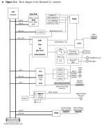
Screen Shot 2019-07-19 at 8.57.49 AM.png

One more thing about the LC PDS and the LC series' address map. The earlier LC PDS machines have a 96-pin connector that does not carry the entire address bus. The LC III and the 68040 LCs added another little connector below to accommodate more address lines (and thus a larger main memory capacity). Looking at the LC's address map, you can see that given a 32-bit address, the device to be accessed can be uniquely identified by A31 and A23..0:

Screen Shot 2019-07-19 at 8.56.36 AM.png

So the consequence is that some signals between A31 and A23 can be left off of the PDS connector. In particular, A31 and A27..A0 are sent to the LC PDS card, with A30..28 excluded.

On an LC PDS card, here is the circuit to generate the card select signal, as you can see, totally independent of A30..A24:
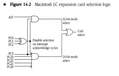
Screen Shot 2019-07-19 at 8.55.27 AM.png

To interface an LC PDS card to an SE/30, the solution goes something like this. We must run in 32-bit mode by tying the LC PDS card's FC3 high. Like the later LCs, the SE/30 only outputs 32-bit addresses onto the bus, as the 24-to-32 translation is done internally in the 68030's MMU. Then we map SE/30 address $FCXXXXXX to $FEXXXXXX on the card by inverting A25. Also, since in 32-bit mode, the selection of the LC PDS card can be done based just on A31, we must also gate A31 such that A31 is 0 when an address not of the form $FCXXXXXX is on the Mac side of the address bus. When the LC PDS card does DMA, we must send back what it drives onto the address bus exactly, with no inversion. We also need to send A30..28 back to the SE/30, since the LC PDS card does not have those pins. DMA devices rarely access peripherals, so we will reconstruct A30..28 as if the LC PDS card is commanding an access to RAM. If we send back all 0's for A30..28 during a DMA transfer, this forces an access into the range of either $0XXXXXXX or $8XXXXXXX. $8XXXXXXX is NuBus extended slot space in the SE/30, which is empty, and also an LC PDS card is unlikely to perform a DMA access with A31 set, since that means the card would be trying to access itself using DMA. $0XXXXXXX refers to the first 256MB of the 1GB assigned to RAM in the SE/30. Since the SE/30's memory controller can only address 128MB, we're good.

I wrote a tiny bit of PALASM which should allow you to accomplish this in a GAL:

Code:
;PALASM Design Description

;---------------------------------- Declaration Segment ------------
TITLE    LC to SE30
PATTERN  
REVISION 0.1
AUTHOR   Zane Kaminski
COMPANY  Garrett's Workshop
DATE     07/19/19

CHIP  _LCTOSE30  PALCE16V8

;---------------------------------- PIN Declarations ---------------
PIN  2          /BGACK                                           ;       
PIN  3          MacA27                                           ;       
PIN  4          MacA26                                           ;       
PIN  5          MacA24                                           ;       

PIN  12         MacA25                             COMBINATORIAL ;       
PIN  13         CardA25                            COMBINATORIAL ;       
PIN  14         CardA31                            COMBINATORIAL ;       
PIN  15         MacA31                             COMBINATORIAL ;       
PIN  16         MacA30                             COMBINATORIAL ;       
PIN  17         MacA29                             COMBINATORIAL ;       
PIN  18         MacA28                             COMBINATORIAL ;       

;----------------------------------- Boolean Equation Segment ------
EQUATIONS

; During DMA, output A30..28 = 0, A25=A25, A31=A31 back to Mac
MacA31 = CardA31
MacA30 = 0
MacA29 = 0
MacA28 = 0
MacA25 = CardA25
MacA31.TRST = BGACK
MacA30.TRST = BGACK
MacA29.TRST = BGACK
MacA28.TRST = BGACK
MacA25.TRST = BGACK

; When DMA not occurring, output inversion of MacA25 to LC PDS card
; and gate CardA31 with MacA==FCXXXXXX
CardA31 = MacA31 * MacA30 * MacA29 * MacA28 * MacA27 * MacA26 * /MacA25 * /MacA24
CardA25 = /MacA25
CardA31.TRST = /BGACK
CardA25.TRST = /BGACK


;-------------------------------------------------------------------


Try compiling that with PALASM in DOSBOX. Maybe there are some mistakes but the idea is right, I think. You could also try to work in a more sophisticated IRQ scheme into the PAL somehow. There is one spare output pin in the GAL16V8 so hopefully you can fit it all in the little GAL. Otherwise try the GAL22V10 or a larger CPLD like an Atmel ATF1500-series or an Altera MAX7000S-series.

 
Last edited by a moderator:
Wait, no, there is a slight problem. I have an idea to solve it. One sec.

edit: fixed. Edits are shown in bold in my previous post.

 
Last edited by a moderator:
@ZaneKaminski Thanks!  Most of that makes sense to me.  And considering I'm not an engineer, that's a good think.  @Trash80toHP_Mini will be busy for the next couple weeks with other projects, but after that we will try to make something happen.  We will let you know what we find.  Thanks again!!

 
I skimmed through this quickly so let me share what I know about this stuff  .  .  .
Thank you so much for sharing. Of course the windmill I was tilting suddenly transformed into a gate through Hadrian's Wall and  .  .  .  [xx(]

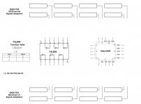
I had been aiming to miss the windmill but the lance sailed straight through the open gate. [:P]   My head has been spinning from re-reading your post now and again for the last few months. The noggin' didn't grok schematics before the collision and it's worse off after it seems. So I fired up AI made a coloring book page!

GAL-Convert-020-to-030-203.jpg

Hopefully you or someone else can connect the dots according to what wraps from where onto where on those two sockets from the signal blocks I've provided for each PDS. A tube of Soldertail GAL16V8 sockets I have on hand and it doesn't look like we'll need anything with more pins? The inverter socket is already on the board if GAL ops don't include inversion of signals.

Any help would be greatly appreciated from anyone. For a translation of the TechSpeak above into n00bish I'd be very grateful.

edit: YAY! My image uploaded, many thanks for your all your hard work @wthww

 
Last edited by a moderator:
Back
Top