• Updated 2023-07-12: Hello, Guest! Welcome back, and be sure to check out this follow-up post about our outage a week or so ago.

SuperMac Spectrum/24 Series III Display Artifact Issue

jmacz

Well-known member
So again, it could be I took a faulty measurement. But it's the following:

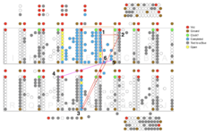
suspect.png
(Sorry for the numbering -- please note that the numbers are just arbitrary and do NOT correspond to chip pin numbers).

While it was in an error state previously, I had recorded in my notes that pin 1 and pin 3 and via 6 had continuity with < 1 Ohm resistance. What I did not have in my notes is that all three of those also had connectivity to pin 2 in the diagram above. I had dragged my probe down that column but either the continuity wasn't there or I had dragged my probe too fast. So I'm going to test the continuity between those pins again once I return to an error state. All of those pins are Data/IO pins.

The other one at least in that area is the connection from pin 4 to via 5. I did not have that one in my notes either. And pin 4 happens to be one that is labeled to be a CLK pin in the GAL spec. But again, as you pointed out, it's not clear this is being used as a clock since only the green pins in that diagram above are all connected and the remaining 8 (of 18 chips) aren't tied to each other.
 

MacOSMonkey

Well-known member
OK. Well... *jeopardy waiting music* :D

Edit: Note that if you find a bad source via on a trace that goes through a secondary routing via, the problem could either be at the pin via or the secondary (especially if within the heating zone).

General Info About Wiring Around Bad Traces (maybe not completely relevant in this case):

Very generally speaking
(and with greater importance in high frequency designs), when wiring around a bad trace, you should try to eliminate any trace stubbing, if possible. For example, if the trace goes to another device pin, then just lift the destination so that the rework wire is the only signal path. Otherwise, if it is an outer layer trace, then you could cut it at the source, destination or an outlet via (leaving enough for a pseudo pad or repair spot for a solder bridge) -- depends on where you need to route. Or, if there is a short hop to a secondary inlet via, you could cut the trace and wire to the secondary via that has a good connection. The point is to try to prevent/minimize dead copper and signal reflections. And, when necessary, you can also terminate traces with resistors where impedance matching matters (such as in the case where you have 50 ohm trace requirements). Wherever there are significant impedance mismatches/junctions, etc., there can be signal reflections that can affect signal integrity. But again, it probably doesn't matter so much for the "Rider" accelerator board for Spectrum/24 Series III -- I am just adding the above for informational purposes.

Caveat: It may go without saying, but...never cut traces unless you are absolutely sure you have the right ones and you are sure of the rework. ;)
 

jmacz

Well-known member
Nice, appreciate that tip. I figure if I am eventually able to identify the pins involved, I will be spending more time under a scope tracing the paths (or attempting to).

Now if I can't find it and there's nothing left but the actual ICs... 😬😱
 

MacOSMonkey

Well-known member
True...and if it's a device via, depending on the clearances and whether or not you have a good drill press, you could also do a very careful drill and force-fill with silver conductive epoxy. Then, you could shorten the device pin so it touches instead of goes through the hole, and it would be an invisible rework. Or, if the via issue were to extend too far beyond the annular ring and the drill and fill didn't work, then you could still just fall back to rework wire.

Also, another tip: with rework, if you have to lift a pin (for whatever reason), try not to bend it at the package/shoulder. It is usually better to just shorten the through-hole lead slightly and carefully j-bend a foot that is above the surface so that you never strain or fatigue the shoulder joint at the package.
 

jmacz

Well-known member
Been a little over a month and thought I'd provide an update.

I could not find any traces with any non-normal resistance. Although I had other projects, I kept coming back to this from time to time to test some more and made zero progress in determining if any traces were bad. Yet heating did temporarily resolve the issue, albeit only for a shorter amount of time now compared to a week before.

I then did something really dumb and I regret it -- but it was due to a growing lack of patience with this card, and with my mind consumed with other projects. I did the following but instead of in a controlled manner, did it all at once:
  • Desoldered six chips in that area (I think previously I had done three) and resoldered them to the board with clean solder.
  • Desoldered the two board connectors and resoldered them to the board with clean solder.
  • Removed 3 capacitors in the area where I have been heating and replaced them with new capacitors.
The three capacitors (ceramic) were marked with "104" which means they should be 100nF. One of them was around 110nF and the other two were closer to 140nF. I would think that should be fine. But as I was holding one of them with a tweezer, it started falling apart (a chunk broke off). I did not think I was holding it that tight. Go figure. I replaced all three with new 100nF ceramic capacitors. These capacitors are sitting between Vcc and Gnd above each and every chip on the board.

I then gave the board yet another IPA bath, brushing, cleaning and installed the board back on the main video card.

Now it's been a few days and so far I haven't seen the issue. Going to keep an eye on it and see if the issue comes back. If it doesn't, that's where I regret making all three changes at the same time because if the problem stays solved, I won't know which one of the three fixed it.

If the issue comes back... well, after pulling my hair out, I might try replacing all the remaining 15 caps. And if that doesn't work, will probably desolder every chip and take another look at the naked board.
 
Top