• Updated 2023-07-12: Hello, Guest! Welcome back, and be sure to check out this follow-up post about our outage a week or so ago.

PowerBook 100 Accelerator Insanity

Trash80toHP_Mini

NIGHT STALKER
Yet another crazy hack that's waaaay over my head  .  .  .  probably! It's looking a bit different with current ProtoBoard technology.

Back in 2013 I got it stuck in my head that my 16MHz 68030 MicroMac Performer might be shoehorned into the Macintosh Portable:

MacintoshPortable Slot Hackage

Back in 2015 techknight got the bug to build a dedicated accelerator for the Portable

mac portable accelerator

Here's the version of the Performer for the SE:


View attachment 19259

Mine's for the Mac Plus, so the EuroDin connector in uninplemented, direct 68000/Killy Klip interface is present and the unimplemented GAL at U7 is populated. This version has the QFP-132 68030 installed where mine is in the standard PGA package.

Total component count on my board for the unbuffered 68000 legs/PDS:

68030

Crystal

5 GALs

68882 Socket

PGA-68 thruholes for who knows what? 68000 PDS passthru?

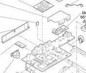
Enter the PB100 processor/ROM/PSRAM (2MB) on the PowerBook 100 Daughtercard:
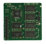
PB100 Daughtercard.png

PB100-Exploded-Daughtercard-RAMcard.JPG

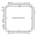
68000 is a smaller QFP, the same as the QFP-132 68030 on the Performer/SE above. The Processor Card is lower than the RAM expansion Card, so the Accelerator could overlap its real estate, providing for the full 8MB RAM allotment for the PB100 on a single daughtercard.

Wasn't sure if the larger QFP-132 would fit in cubic underneath the board occupied by the QFP-68 68000, but found that may not matter.

There's a KBD support on the solder side of the PB-100 Daughterboard which may indicate that there is room to do a double sided design providing somewhere between 250% and 300% of the original PCBs single sided real estate. There are also SMT Pads for the two board interconnects on the solder side of the Daughterboard indicating that stacking another PCB on top of it may have been considered.

Dunno, we'll see. The SE/Plus/Classic Performer doubles the host's clock, raising the local bus of the 68030 to 16MHz.

The PB100 clock is already at 16MHz. ROM & RAM look to be located on the Daughtercard's local bus. Enter the MC68030FE33B-QFP-132:

MC68030FE33B-QFP-132.jpg

@tk: these puppies have gone down to $14 ea. on eBay. [:D]

Insane WAG of the week would be that the proposed 68030 PowerBook 100 Accelerator would be running at 32MHz and that ROM and RAM would be along for that faster ride on its local bus?

Dunno, is there a memory controller on the PB100 main board? Moving the five existing GAL ICs to the prototype would seem to be the thing to do. Maybe tweak the oscillator value? Might the same clock on the accelerator also double the 16MHz rate of the host?

Coffee's kicking in so I'm losing my train of thought. :blink:

33MHz 68030/68882 FPU/8MB RAM infused PowerBook 100 anyone?

Comments please!

edit: forgot to mention that it would appear that none of the limitations of the Portable's PDS are present on the board interconnects of the PowerBook 100 CPU/ROM/PSRAM daughterboard. [:D]

edit: one last thing, since the native 68000 the Performer's Driver needed to disable would be missing from the accelerator, might the 68030 accelerator "just work" as is the case for a Sonnet CrescendoPB's G3 accelerator replacement of the 1400's Processor Daughterboard? Avoiding INIT/Driver foibles would be very cool indeed! Potentially a far more simple prospect than adapting the Performer setup to the Portable's PDS.

 
Last edited by a moderator:

Trash80toHP_Mini

NIGHT STALKER
Been flipping the building blocks around in the noggin again this fine AM, came up with a few of notions for testing:

- desolder and socket the 68030 and crystal on the Performer.

- - - swap in the 40MHz 68030 from the DOA 840AV

- - - determine crystal necessary to quadruple the 8MHz bus of the Plus

I can then test the accelerator to see if it will function on a 32MHz Local Bus for the 68030

- the only active components on the Performer are the GAL16V8B ICs.

- the GAL16V8 (same specs?) data sheet seems to say it will run at 166MHz max.

- that data sheet says it's CMOS so one hiccup might be down  .  .  .  hopefully:

Gorgonops's comment on the Portable Hack proposal:

Another minor point is the Mac Portable is all CMOS, whilst I *believe* all the desktop Macs listed were still using TTL-level circuitry. The developer note doesn't mention difference in voltage levels, but there's a non-trivial possibility that even if the clock speed differences aren't a problem (and I wouldn't underestimate the chances of that) if there's TTL circuity on that card it may not reliably drive the portable's bus.


So let's see:

- Is it safe to assume that the earlier PGA 68030 is CMOS? Gotta dig out that data sheet.

- I can't imagine the 33MHz QFP part wouldn't be? I'm guessing that if I pull the PB150 apart that's what I'll find?

- Will I find a different, low power version of the QFP part pictured above in the 100 series PowerBooks?

I've got an extra SE board to play with to test another possible problem:

- desolder the DIP 68000

- install socket

That'll let me mate the Performer with the SE as if it were the plus using headers for the F-F socket conversion. That'll let me test my CrescendoPB, "it just works" hypothesis:

WAG: without the logic board's 68000 to disable, the Performer's 68030 will boot from ROM at startup without need for its INIT/Driver?

What test procedures an I missing here?

End game - If the above tests are positive:

- desolder the QFP 68000 on my spare PB100 daughtercard

- patch wire its pads to a another 68000 DIP socket hot glued to the (upper) solder side of the daughtercard

- guessing I'll need to patch power and ground of the socket to the main board to run the Performer?

- repeat testing procedures above.

What's obviously wrong about this approach to the problem set? :blink:

 
Last edited by a moderator:

Trash80toHP_Mini

NIGHT STALKER
Even if I can get this crazy contraption to run, the major hurdle will be reverse engineering the GAL formulas. My guess is that their functions could be done by a more capable, single, modern SMT packaged programmable logic IC?

If everything falls into place, might a tiny SEEED board rebuild of the performer be wedged onto the pads for the 68000 in the Portable? :ph34r:


Bolle

Well-known member
Those equations usually are pretty basic. There existed a DIY project from german c't magazine that was about building a 030 accelerator for 68000 machines.

They had GAL sets for the Amiga as well as the Mac. All the documentation on those is found on the web somewhere.

Pretty sure if you compare the GAL connections on their board and on most of the commercial accelerators you will see that they all have a lot in common.

Your Micromac should always work in 030 mode even without the INIT - at least all my 030 accelerators for the SE and Classic do.

Disabling the 68000 is done the same way as the onboard 030 is disabled on 030 PDS/Cache upgrades. Pretty sure you won't need a 68000 at all for the upgrades to work.

The logic can be done in a modern PLD. Just look up the TerribleFire. That thing actually should not be too hard to be modified to work in a Mac - minus the onboard DRAM which is software activated on the Amiga I think.

SRAM could be implemented with some cache logic instead to speed things up. How cache is hooked up to the 030 bus is also well documented on the net somewhere, including needed GAL code and everything... I have it backed up somewhere in my 030 accelerator folder that is hiding somewhere.


Trash80toHP_Mini

NIGHT STALKER
Nice, THX! 32MHz 68030/CoPro AND cache in the PowerBook 100 and Portable would be insane! [:D]

I'm ordering a set of DIP sockets for the SE to test without the CPU, that'll let me box up the project until they arrive from China.

68HC000 in the Portable looks easy enough to wedge. [}:)]


aplmak

Well-known member
The only thing about the 100 compared to the portable is the crappy screen on the 100.... It doesn't compare to the active matrix on the portable..


techknight

Well-known member
I stopped at the point where adapting an 020 or better to an 000 bus requires conversion logic. SIZ0 SIZ1, A0, A1, etc has to be decoded into UDS/LDS, As well as VPA/VMA/E. 

Then there is also negotiation logic needed to force the on-board CPU into High-Z. 


Trash80toHP_Mini

NIGHT STALKER
I'm looking at excising the onboard CPUs, so High-Z/whatever will be a moot point if my approach works at all. The GALs on the performer take care of that bus conversion and it looks like there's plenty of prior art to snag from the Amiga fanatics. It'll be nice to be able to co-opt some of their engineering, that gang makes me look sane! :blink:

Sockets should be here in a month. Yippee Ki-Yay, Somethingorother, poppa's got a brand new bag! [:D]

The only thing about the 100 compared to the portable is the crappy screen on the 100.... It doesn't compare to the active matrix on the portable..
Dunno about that:

1 - my NASA Portable's LCD isn't backlit

2 - my firstest ever, brand new NoteBook's passive LCD is (I'm in the process of rebuilding it)

3 - its LCD matches the far more expensive PowerBook 140's passive LCD in quality, if not in size

4 - the tilt base of BabyPB's LCD weighs about 1.7 lbs. less than the 140's

Should I even bother going into the fact that the NASA Luggable display nook needs an auxiliary shelf support? :lol:


Trash80toHP_Mini

NIGHT STALKER
Forgot to mention that combinatorial bits will be making up the required 68pin sockets. Anybody seen wide 68pin DIP sockets anywhere?

edit: never mind, ordered some 40 and 28 pin sockets to chop up. they'll be used as strips to plug into machine pin header strips soldered in place of the CPU of the SE. :ph34r:

 
Last edited by a moderator:

Trash80toHP_Mini

NIGHT STALKER
Sat down for my morning coffee/posting ritual and decided to review this mess, found some booboos to correct:

Correction stuff:

It's the RAM expansion slot that's lower than the CPU daughtercard slot in the PowerBook 100.
____ so the daughtercard to be enlarged such that it overhangs the an empty RAM expansion connector.

This could be important for a couple of reasons:
____ additional real estate on the accelerator is good
____ upping the daughtercard/accelerator's memory from the standard board's 2MB to the full 8MB allotment is better!
________ BabyPB has the 6MB maxed memory expansion card, but they're scarce as hens teeth, sooo  .  .  .  [}:)]

gorgonops, I got your CMOS warning all wrong, but it may not matter:
____ GAL16V8B ICs on the Performer are CMOS and you'd said they might not drive a host's TTL logic adequately.
________ They're a bi-directional(?) interface between the 68030/68882 combo and Plus or better 68000 parts.
____________ if so: the Plus CPU must be CMOS along with the 68030/68882?
____________ therefore no problem(?) = no CMOS<->TTL driver IC requirements?

Still gotta dig up those Data Sheets.

New stuff:

Ordered a pair of the  MC68030FE33B-QFP-132 CPUs listed above, they won't go to waste even if nothing comes of this project:

I have several IIsi boards on hand and their 20MHz CPUs could use a boost. Word on the street is that the IIsi MoBo was designed to run at 25MHz. With a 33MHz CPU on board overclocking might be interesting!

Also ordered an untested IIci board for testing my 50MHz PowerCache. I'm wondering at what point overclocking will break the IIci with a 33MHz CPU on board. :ph34r:

 
Last edited by a moderator:

Trash80toHP_Mini

NIGHT STALKER
New questions:

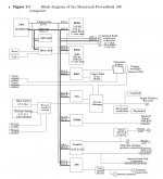
Per the DevNote Block Diagram, memory resides on the processor bus with no memory controller present.

  --Will the 68030 handle memory in the same fashion?

 --Might more modern memory be substituted for the PSRAM?

 --Might a LOT of memory be addressed by by the 68030 with its PMMU on board?

 --Might Compact virtual or the like work on PB100 and Luggable? [}:)]


techknight

Well-known member
Would be nice if I had the code for the Xilinx XC series CPLDs to handle the bus conversion logic. like the XC9536 or XC9572 as those I am familiar with. 


Trash80toHP_Mini

NIGHT STALKER
I think I'm just going to go ahead and install machine pin socket strips I have on hand instead of waiting a month to behead an SE board.

Good news on the data sheet front, earlier versions of the 68000 were HMOS, but the 68HC000 low power chip in the PB100 daughtercard and Luggable is CMOS. Interesting reading, as compared to the vanilla 68000, the 68HC000 is a much more capable CPU.

RAM and ROM are right on the processor bus of the PB100:

PB100-block_diagram.JPG

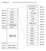
PowerBook100-Memory_Map.JPG

Still trying to figure out the addressing setup, 19 bits to access so little ROM & RAM?

Will the 32bit addressing of the 68030 let the likes of Compact Virtual use up to 32MB of additional RAM as other 68030 based Compact Mac accelerators?

@tk: I took a peek at Amiga stuff online and saw that XC prefix more than a few times IIRC. What the heck happened to make the Terriblefire accelerator developer pack it in?


Trash80toHP_Mini

NIGHT STALKER
The insanity begins! Just finished buzzing out the odd side of the daughterboard connector. The interconnections between it, CPU, ROM and PSRAM are half done. Nothing unusual to report at this stage. Took a quick look at the Memory Card Slot, didn't expect its signals to line up with the daughtercard connector's pinout, no joy or disappointment there, they didn't.

There are a few pins coming up from the logic board to the daughtercard that are connected to sections of memory but not to the CPU. I figure that will turn out to be CPU GLU acting as a rudimentary memory controller, we shall see. That jibes with the low pin counts, both have 70 lines with an additional 10 lines on a second connector between the CPU daughterboard and the main board.

Most of the Bank Select/RAS/CAS lines will be heading up the memory side of the connector pair to control the 6MB of expansion memory however it's arranged overall. If so, that'll complicate things for putting all 8MB on the daughtercard.

Gotta get the QS'02 set back up to work on the schematic after I finish buzzing the rest of the board in the morning  .  .  .  maybe. :blink:


Trash80toHP_Mini

NIGHT STALKER
Are there schematics of the Portables floating around the web anywhere? Guessing there's not one for the PB100?

Given the memory bank setup of the SE and the bumps in the RAM expansion path, I'm thinking four banks of 2MB in the Portables and PB100?

A look at the signals on the memory expansion slot in the DevNote would have satisfied my curiosity about it being a mirror of the CPU cars slot, but poking around with the meter was more fun, quickly done and I didn't have to get up from the bench. Lazy mode sometimes pays off. Now that I've taken a look at the docs, I figure it'll be easy enough to noodle out pin assignments for the direct connections from main board to ROM and RAM on the CPU card.

Musings about moving memory expansion to the daughtercard took a real hit, but still possible in The Rube Glodbergian 'verse, but it's probably a lot less work and more reliable to just build a new 6MB card as a side project. More folks will want one of those than a crazy accelerator board anyway. I don't need one, but it'd be a fun project for somebody.

Has anyone got any ideas about substituting a more current/available form of memory for the PSRAM.

@tk: curious about how your experience with Memory Expansion for the Portable(s) might apply?  A Reader's Digest Condensed version of anything applicable here would be much appreciated. PSRAM sounds convenient, but dumbing the PB100/Backlit Portable PSRAM setup back down to standard SRAM used in the first Portable (henceforth referred to as the Luggable) seems like it might make it a lot easier to substitute a high density (currently available?) IC?

Splitting something with 8MB or more on a 32 bit data bus would waste some or many chunks of that capacity on both sides of the Bank divide, but be easily split into the four(?) 16 bit 2MB(?) banks of PSRAM of the PB100/Backlit Portable?

Anybody got any notions at all about the refresh method gymnastics involved in converting the auto refresh setup of PSRAM to a real SRAM setup? Was PSRAM a less expensive option than just sticking with SRAM back in the day? SRAM doesn't need a refresh at all, right?

Hope this can be parsed, I may miss the edit window. Gotta clean up a big mess and wake up, I managed to run Mr. Coffee with the carafe sitting on the counter next door once again. :wacko:

edit: anybody know what the interboard connectors are called and if they're still available?

 
Last edited by a moderator:

Trash80toHP_Mini

NIGHT STALKER
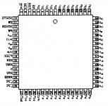
Finished buzzing out the even numbered side of the Daughterboard interconnect and couldn't get the pinouts to line up correctly, then i noticed there weren't any ground pins on the Hitachi HD68HC000 pinout I'd been using! :eek:

HD68HC000-QFP-pinout.JPG

Found the Freescale M68000 manual. Is Vss equivalent to GND somehow?

MC68HC000-QFP-Pinout.JPG

This pinout doesn't freak me out and the real deal's a lot cleaner than that nasty scan. [:p]


techknight

Well-known member
The RAM needs to be as wide as the bus, and then you need to have a CPLD handy for bank switching for the proper addresses. If the RAM is on board the accelerator card and it overrides the RAM on the system board, then you need even more decoding to "tristate" the card on the system bus during RAM read/write access, so it doesn't conflict with the on-board RAM. Extended RAM that isnt on board is fine obviously. 

Good thing is, the RAM could be connected to the 030, and used in 030 style decoding. Dont need the UDS/LDS 16-bit switching as needed on the standard bus, so it would be wired behind that logic. 

But then you still need to handle ROM Overlay at the RESET vector with the RAM on board the accelerator. Dunno how to do that. 

 
Last edited by a moderator:

Trash80toHP_Mini

NIGHT STALKER
Luckily there's zero RAM on the system board, the stock 2MB config is on the CPU daughtercard with the ROMs.

If you're saying the 68030 can use memory directly connected to its bus without a memory controller we're good to go for however much memory we'd like to put on the board.

Thankfully the pads for the SMT connectors on the daughtercard are duplicated on the topside.

Current thinking is to simply lift the Vcc leg of the 68HC000 to disable it and wire up a DIP header kluge for socket interface to the Performer. Likely won't be all required signals, but balance could be patched from the pads on the disabled CPU on the underside.

I'll install the jumper/header power kluge from the DuoDock DeclROM cutout hack so I can power up the Daughtercard's CPU to make sure I haven't borked anything periodically.

To keep things tidier, I can install header sockets in the Performer's PGA interface for the Classic version's connector.

__ that would give me a standard header/socket interface that will more easily fit a 10cm x 10cm adapter board

____ installing the sockets or headers on the top to mount the Performer upside down leaves the bottom unobstructed

______ if I manage not to kill the thing I can put it back into my Drexel/Plus

____  I may have found SMT sockets to install on top of the Daughtercard

______ Looks like they'll clear the bottom of the keyboard  so I can still use it if I can avoid killing it.  :wacko:

I'll power everything on the 68000/Performer interface from the HDD connector.

Feedback on that 68030 memory mode thing would be very much appreciated. I'll have to check the manual, but you might be able to save me a lot of effort there.

How does this approach to basic feasibility testing sound overall?

Is there any applicability of any of this to your Portable Accelerator project?

 
Last edited by a moderator:

Trash80toHP_Mini

NIGHT STALKER
Would be nice if I had the code for the Xilinx XC series CPLDs to handle the bus conversion logic. like the XC9536 or XC9572 as those I am familiar with. 
I've been poking around some and it looks like we might be able to implement that bus conversion logic, the 256K ROM and a memory controller to interface the 68030 with onboard non-PB100 memory.

In such a case we shouldn't need whatever the Logic board may be doing in terms of acting as a memory controller for main and expansion memory banks. How much of this kind of crud can we fit on a CPLD?

How do 68030 accelerators for the SE interface with the SIMMs on board?

Should Compact Virtual be able to run on any 68000/68030 combo? There was never any way/reason to test in on the PB100 or the Portable?

 
Top