• Updated 2023-07-12: Hello, Guest! Welcome back, and be sure to check out this follow-up post about our outage a week or so ago.

Lobos board (Strange Apple ROM)

Phipli

Well-known member
One hardware difference I can see is that the djMEMC is a different part number than usual, it is VY16568-2 instead of just VY16568, but that may just be denoting the revision.
That might be related to the issues I was having. I had my 650 set to the unreleased 40MHz machine ID, this adjust various multipliers so that when you drop in a 40mhz clock, the video isn't overclocked. The one issue I had was that the machine became more picky about RAM and I had to remove the SIMMs I was using and swap them for others. The ones I removed were technically fast enough, so... ah well.
 

switch998

Well-known member
The ROM is indeed different. CRC32 is 3318a935 on this one.

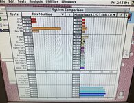
I used speedometer to measure the results. Not sure how good these look since I don't have a retail 33mhz Q800 to compare against
 

Attachments

  • Quadra_800_40Mhz-EVT2.ROM.zip
    480 KB · Views: 9
  • IMG_0582.jpeg
    IMG_0582.jpeg
    3.1 MB · Views: 16

Phipli

Well-known member
The ROM is indeed different. CRC32 is 3318a935 on this one.

I used speedometer to measure the results. Not sure how good these look since I don't have a retail 33mhz Q800 to compare against
Excellent, thank you!

I just need to swap my dad's 650 with mine now, his has a ROM slot :)
 

cy384

Well-known member
thanks for sharing this!

from an extremely brief look, it seems like: some change to the CPU detection code, something in the djmemc setup, some other stuff I don't have mapped out, and the date is changed 12th of november, 1993

the changes are pretty small, like 500 bytes difference, mostly in one area

(this is relative to the Q800 F1ACAD13 ROM)
 

cy384

Well-known member
oh, btw, I wrote a little program to inspect the djmemc (memory controller) settings, at some point hopefully I'll have time to burn this ROM and test it out on my machine, if anyone else wants to try, I've attached it (as mac binary)

there's some discussion related to this tool over in the wombat overclocking thread
 

Attachments

  • ultra-wombat-hax-tool.bin
    128.6 KB · Views: 1

cy384

Well-known member
I tried running this ROM in my machine, which is basically a Quadra 650, but it set up the memory controller exactly the same as the stock ROM. I believe it may be looking for a different gestalt machine ID; mine is set up to report being a 36. The prototype machine may be the elusive gestalt ID number 51. If someone with one of them can check and/or run the tool I wrote (previous post) that would be very cool!
 

cheesestraws

Well-known member
Yeah, I'd expect it to be looking for a gestalt ID - ISTR in the stock ROM the memory controller setup table is parameterised by gestalt ID, it seems reasonable to expect the pre-release ROM to be as well.
 

Phipli

Well-known member
I tried running this ROM in my machine, which is basically a Quadra 650, but it set up the memory controller exactly the same as the stock ROM. I believe it may be looking for a different gestalt machine ID; mine is set up to report being a 36. The prototype machine may be the elusive gestalt ID number 51. If someone with one of them can check and/or run the tool I wrote (previous post) that would be very cool!
Details on how to get the unreleased Gestalts here :


Jockelill

Well-known member
Was this ROM ever dumped? Otherwise both me and @WillJac are building ROM programmers and have sold a few already in UK. I'm based in Sweden and happy to help out if I can borrow that ROM.
 

eharmon

Well-known member
The ROM is indeed different. CRC32 is 3318a935 on this one.

I used speedometer to measure the results. Not sure how good these look since I don't have a retail 33mhz Q800 to compare against
Unfortunately this is just a Centris 650 ROM, presumably the Quadra 800/650 changes hadn't been put in place yet.

Centris 650 ROM checksum: 0xF1A6F343
Quadra 800 EVT 2 ROM checksum: 0xF1A6F343

I do wonder what makes that a 40MHz board...maybe it was reworked later to switch to the 33MHz board ID to downgrade it. But knowing the part specs would be helpful for "officially" modding a retail board to 40.
 

Phipli

Well-known member
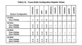
A 40MHz 650 would ideally have 60ns onboard RAM, and a MC88916DW80. Then you need a 40MHz CPU and appropriate CPU clock, and move the resistors around to tell the ROM to use 40MHz timings by setting the gestalt to the unreleased 650 or 800 (51 or 59).
Unfortunately this is just a Centris 650 ROM,
Note my 650 that I do all my messing with overclocks and the 40MHz timings with is a Centris.
 
Last edited:

eharmon

Well-known member
A 40MHz 650 would ideally have 60ns onboard RAM, and a MC88916DW80. Then you need a 40MHz CPU and appropriate CPU clock, and move the resistors around to tell the ROM to use 40MHz timings by setting the gestalt to the unreleased 650 or 800 (51 or 59).

Note my 650 that I do all my messing with overclocks and the 40MHz timings with is a Centris.
Right, I meant that, since it's actually labeled as a 40MHz board, maybe we could see the full set of "correctly" spec'd chips from factory. They're probably exactly the specs suggested, but it's interesting to know definitively what was planned. Sometimes there are surprises!

(FWIW, based on the tables I believe the bump40 configs do not require 60ns memory -- they're tuned for 80 -- but the "regular" configs do expect 60ns and run faster as a result. I think it's been overlooked a few times, but there's two sets of tables and the configurations match those speeds, respectively.)
 

Phipli

Well-known member
Right, I meant that, since it's actually labeled as a 40MHz board, maybe we could see the full set of "correctly" spec'd chips from factory. They're probably exactly the specs suggested, but it's interesting to know definitively what was planned. Sometimes there are surprises!

(FWIW, based on the tables I believe the bump40 configs do not require 60ns memory -- they're tuned for 80 -- but the "regular" configs do expect 60ns and run faster as a result. I think it's been overlooked a few times, but there's two sets of tables and the configurations match those speeds, respectively.)
Sorry, my bad, I googled a Q800 board knowing the djmemc only recommends the higher speed between the 650 and 800 for 40MHz, but the board I found had 60ns chips. Actually checking properly I see the Q800 probably only actually needs 70ns and the 60ns fitted in the photo were likely an over specification substitution.

1000014980.jpg

So yes, 70ns is fine, but some C650s are fitted with 80ns.
 
Last edited:

Phipli

Well-known member
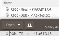
Folks, I just ran unirom on the prototype ROM and it has the same ROM ID as the early production 650 / 800 ROM, so it is just one of the two production ROMs.

Note the 40MHz prototype board is dated... August 1992 - the Centris 650 and Quadra 800 were released in Feb 1993, so this machine is just them testing the board at 40MHz before they went on to spectacularly... not release a 40MHz version.

Sadly this means we're not going to get any timings we didn't know about from the prototype ROM and it isn't updated hardware.

The F1ACAD13 ROM (the updated wombat ROM) might be more interesting though?

1703871315132.png

The line in the text file (under "Open") is the prototype ROM.
 

eharmon

Well-known member
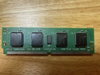
My new toy arrived today, what looks like a 4MB version of the Lobos board, with part number AP2633-01:

IMG_2170.jpeg

It's got 8x AM29F040B.

@dougg3, what would you need to add support for the SIMM programmer? I successfully read out part of the ROM by using 4x 8Mb, but as you'd expect that only got me half the bits.
 

dougg3

Well-known member
It's got 8x AM29F040B.

Ooh, very interesting! Thanks for sharing! I find this fascinating because AM29F040B doesn't require VPP, and also isn't supported by Apple's Flasher app I disassembled. These chips will identify itself as manufacturer ID 0x01 and device ID 0xA4. That combination is nowhere to be found in Flasher. Several 28F020 variants are supported, but nothing for 29F040. But clearly your picture shows AM29F040B. I'm intrigued.

Each chip is 512 KB so this is a 4 MB SIMM, which I'm guessing you already knew based on the "4MB PLCC FLASH SIMM" silkscreen and of course the chip datasheet.

Since this is an Apple SIMM I expect you will find that /WE is on pin 3 of the SIMM connector rather than the pin I chose for the SIMM programmer (13), so it's likely that it won't ever be flashable in my programmer, unless they happened to hook /WE up to pin 13 like I did. I feel like you should be able to read the entire content through the programmer by just saying you have a 4 MB SIMM inserted though -- for example the 4MB (4x 8Mb PLCC) option like you said. I actually do expect that to read all of the content because I would expect it to be hooked up to the Mac address bus the exact same way my programmer would read it out.

Do you happen to be really bored? It would be awesome if you could trace out exactly how things are connected. I suspect the data bus D0-D31 is going directly to each set of 4 chips. Like 2 chips are hooked to D0-D7, 2 chips are hooked to D8-15, and so on. I also expect most of the address bus (A2-A20) to go directly to all eight chips. U9 (in conjunction with any other special additional chips) is probably responsible for generating /OE and /WE signals based on the original /OE and /WE signals along with another address line, like A21. I guess it's also possible they did the logic using A2, but that would interleave the data weirdly.

Would you be willing to take some closer pics of both sides of the board with all the chip markings readable? I'm especially interested in what's going on with U9, and what part number is on it. Is there another chip on the other side of the board too? I suspect it's going to be some logic gates to decide which half of the SIMM to activate. My guess is the logic will be something along these lines:
  • U1-U4 /OE = /OE OR A21
  • U1-U4 /WE = /WE OR A21
  • U5-U8 /OE = /OE OR ~A21
  • U5-U8 /WE = /WE OR ~A21
...but that's just a somewhat educated guess. I could also be way wrong. I feel like there would probably have to be one more chip to implement the logic I just described, unless it's a PAL instead of a 74 series chip.

It's probably possible to hack Flasher to support this SIMM for in-system programming. I'm kind of surprised to see an Apple SIMM with this type of flash chip on it, but based on the date on the board it came later so I guess it makes sense. There must be a newer version of Flasher out there somewhere that supports it. I don't see support for it in the TNT Flasher either, which is the newest I've seen so far.
 

eharmon

Well-known member
Ooh, very interesting! Thanks for sharing! I find this fascinating because AM29F040B doesn't require VPP, and also isn't supported by Apple's Flasher app I disassembled. These chips will identify itself as manufacturer ID 0x01 and device ID 0xA4. That combination is nowhere to be found in Flasher. Several 28F020 variants are supported, but nothing for 29F040. But clearly your picture shows AM29F040B. I'm intrigued.

Each chip is 512 KB so this is a 4 MB SIMM, which I'm guessing you already knew based on the "4MB PLCC FLASH SIMM" silkscreen and of course the chip datasheet.

Since this is an Apple SIMM I expect you will find that /WE is on pin 3 of the SIMM connector rather than the pin I chose for the SIMM programmer (13), so it's likely that it won't ever be flashable in my programmer, unless they happened to hook /WE up to pin 13 like I did. I feel like you should be able to read the entire content through the programmer by just saying you have a 4 MB SIMM inserted though -- for example the 4MB (4x 8Mb PLCC) option like you said. I actually do expect that to read all of the content because I would expect it to be hooked up to the Mac address bus the exact same way my programmer would read it out.

Do you happen to be really bored? It would be awesome if you could trace out exactly how things are connected. I suspect the data bus D0-D31 is going directly to each set of 4 chips. Like 2 chips are hooked to D0-D7, 2 chips are hooked to D8-15, and so on. I also expect most of the address bus (A2-A20) to go directly to all eight chips. U9 (in conjunction with any other special additional chips) is probably responsible for generating /OE and /WE signals based on the original /OE and /WE signals along with another address line, like A21. I guess it's also possible they did the logic using A2, but that would interleave the data weirdly.

Would you be willing to take some closer pics of both sides of the board with all the chip markings readable? I'm especially interested in what's going on with U9, and what part number is on it. Is there another chip on the other side of the board too? I suspect it's going to be some logic gates to decide which half of the SIMM to activate. My guess is the logic will be something along these lines:
  • U1-U4 /OE = /OE OR A21
  • U1-U4 /WE = /WE OR A21
  • U5-U8 /OE = /OE OR ~A21
  • U5-U8 /WE = /WE OR ~A21
...but that's just a somewhat educated guess. I could also be way wrong. I feel like there would probably have to be one more chip to implement the logic I just described, unless it's a PAL instead of a 74 series chip.

It's probably possible to hack Flasher to support this SIMM for in-system programming. I'm kind of surprised to see an Apple SIMM with this type of flash chip on it, but based on the date on the board it came later so I guess it makes sense. There must be a newer version of Flasher out there somewhere that supports it. I don't see support for it in the TNT Flasher either, which is the newest I've seen so far.
I can trace things out later this week, but some quick updates to your other questions:

Without toning things out I can see one trace on the top layer going from pin 3 to /WE, so I bet it is the same as other Apple flashable ROMs.

It might require a new rev, but it would be nice to use those directly on the ROM programmer next time around...for all 4 of us with Apple programmable ROMs!

U9 is a 74F86D. There are no other chips, just capacitors for each flash chip.

Reading the chip with any of the 4MB settings yields every 4 bytes missing. For instance, I find the string:
Code:
Adoystencorted

Which I believe should be:
Code:
Adobe Systems Incorporated

So we have:
Code:
Adobe Systems Incorporated
AdoXXXXysteXXXXncorXXXXted

Which yields my conclusion it's only reading half the data. I do get a 4MB read though with data throughout, so I wonder if the data has just been flipped to another section of the file?

Trying to ID the chips doesn't seem to work. I get data back but it seems bogus, different for all the chips. It seems like the firmware might be hardcoded to only read 4 chips worth of data? I only skimmed the code though:
Code:
IC1: 0x06 / 0x5C
IC2: 0x00 / 0xDD
IC3: 0x00 / 0x01
IC4: 0xA0 / 0x00

And a question you didn't ask, I found copyright dates of 1997...so this must be very late Old World. I wonder if Power PC can do in-system flash as well, then.
 

dougg3

Well-known member
It might require a new rev, but it would be nice to use those directly on the ROM programmer next time around...for all 4 of us with Apple programmable ROMs!

It seems like it wouldn't be too bad to optionally put /WE on pin 3 instead of 13, but optionally putting 12V onto pin 2 would be a bigger challenge. Not relevant for your SIMM which doesn't need VPP, but would be relevant for the Lobos board. It's not something I will have time to do in the near future, but maybe someone will...

U9 is a 74F86D. There are no other chips, just capacitors for each flash chip.

Thanks! So four XOR gates. If you're seeing pin 3 go directly to /WE on a chip, I'm guessing /WE and /OE go direct to the chips and the 74F86D is generating /CE for the two banks of 4 chips. That's probably doable with some XOR magic on the address pins or something.

Reading the chip with any of the 4MB settings yields every 4 bytes missing.

I have a few random ideas. You should check to make sure the entire 4 MB readback is unique data, and not two repetitions of the same data. If it's unique data, you likely have an entire dump of those chips. If there are two repetitions of the same data it could indicate we're only getting half of the total 4 MB of contents (I don't think this is possible though). Also, have you checked to see if the missing XXXX data is elsewhere in the dump, like maybe exactly 2 MB afterward? Maybe it's just arranged weirdly.

Now that you mention 1997 though, I agree -- 1997 date screams PowerPC to me. PowerPC Macs have a 64-bit wide ROM data bus. I wonder if you need two of these SIMMs to fill the data bus? Maybe some early dev board had two 64-pin ROM SIMM sockets, or maybe there was a DIMM adapter board that took two 64-pin SIMMs and plugged into the PowerPC ROM DIMM socket. That seems kind of far-fetched, but it would explain every other set of 4 bytes being missing. I still think this sounds crazy, but the 64-pin SIMM isn't really suited for PowerPC because it only has half as wide of a data bus as needed. Is it possible this SIMM came from a pair where the other SIMM contains the other half of the missing data? That would be 8 MB of total data though, and all the PowerPC ROMs were 4 MB. But I still don't see how this single 4 MB SIMM could be used in a PowerPC by itself because it would need to provide 64 bits of data simultaneously during each read cycle.

Trying to ID the chips doesn't seem to work. I get data back but it seems bogus, different for all the chips

This generally means the unlock sequence being written isn't correct for the chips so they're just returning data near the start of the chip instead. However, the SIMM programmer definitely uses the proper unlock sequence for the Am29F040B because I played around with that exact chip when I was first getting started with programmable SIMMs.

I think there are two separate reasons that chip ID isn't working for you:
  1. Identification requires write cycles, and /WE is probably on the wrong pin for compatibility with the SIMM programmer.
  2. Even if /WE was wired correctly, there's another problem. Because there are 8 chips and only 32 data bits, something has to be a bank select -- probably one of the address pins. I wouldn't want to be toggling that address bit during the unlock sequence. It would need to stay constant during unlocking, write cycles, read cycles, etc. when I'm trying to deal with a specific bank. Right now the programmer firmware would definitely not be meeting that requirement. The programmer firmware would have to be updated to know how to program SIMMs with multiple banks like this.

I wonder if Power PC can do in-system flash as well,

They definitely can, at least some of them. I never saw any with 64-pin SIMM sockets though (you'd need two of them for 64 bits of data), which is why I'm slightly puzzled and wondering if there was an adapter board or something...

Very interesting stuff though. I'm definitely curious how it's wired up when you get a chance to check it out. I think seeing the inputs and outputs of the XOR gates will answer some questions for us. My guess is one of the gate outputs goes to /CE on U1-U4 and another goes to /CE on U5-U8. Once you've traced it out we can figure out how it all works.
 

eharmon

Well-known member
Now that you mention 1997 though, I agree -- 1997 date screams PowerPC to me. PowerPC Macs have a 64-bit wide ROM data bus. I wonder if you need two of these SIMMs to fill the data bus? Maybe some early dev board had two 64-pin ROM SIMM sockets, or maybe there was a DIMM adapter board that took two 64-pin SIMMs and plugged into the PowerPC ROM DIMM socket. That seems kind of far-fetched, but it would explain every other set of 4 bytes being missing. I still think this sounds crazy, but the 64-pin SIMM isn't really suited for PowerPC because it only has half as wide of a data bus as needed. Is it possible this SIMM came from a pair where the other SIMM contains the other half of the missing data? That would be 8 MB of total data though, and all the PowerPC ROMs were 4 MB. But I still don't see how this single 4 MB SIMM could be used in a PowerPC by itself because it would need to provide 64 bits of data simultaneously during each read cycle.
Ack on the other items, will follow-up tomorrow or later this week because I’m super curious too.

But I’ve determined you’re 100% right. Looking much closer at the smudged sticker on the back it says “EVEN”…and the picture the seller provided says “ODD”!

So I’ve got half an 8MB ROM. Weird!

I contacted the seller to see if they happen to still have the ODD one…if not…if anyone stumbles upon this thread looking for more details on a mystery 4MB PLCC Flash ROM they purchased, by combining our dumps we can find out what’s on it!
 
Top