• Updated 2023-07-12: Hello, Guest! Welcome back, and be sure to check out this follow-up post about our outage a week or so ago.

IIsi PowerCache TwinSlot Adapter - Cloning Project

Trash80toHP_Mini

NIGHT STALKER
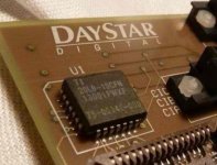
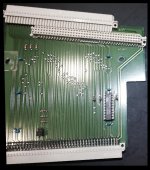
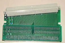
Noticed something strange about what appear to be connections between the FPU pads and the GAL(?) adapter IC on this board. Since there's an SE/30 Adapter Cloning Project, a dedicated  thread concerning this facet of the overall PowerCache Adapter Cloning Project seems in order. Lines of research are beginning to get muddled. ::)

View attachment 11264

This PCB is a humdinger! There are traces visible on subsurface layers on both sides of this four(?) layer board.

edit: any help in buzzing connections on this card would be a significant contribution and greatly appreciated.

 
Last edited by a moderator:

techfury90

Well-known member
The FPU pins in question seem to be CS and RW on the bottom side, A1 and A4 on the left, and top seems to be SENSE, D0, and D3. I suspect there's more hidden through vias. It seems that the GAL may be handling the decode/select function for the 68882 coprocessor interface, as blatantly evidenced by the fact it has something connected to the 882's CS input.


Trash80toHP_Mini

NIGHT STALKER
I was thinking along the lines of the FPU just hanging out on the system bus and the GAL monitoring some signals from its pads in order to tweak the address space of the IIci Slot adaptation. Dunno, maybe some help will be offered tin clearing a few things up.


techfury90

Well-known member
It could be doing both. I question why it's actually running some of those lines to FPU pads. That may have just been a case of something making the design easier by preferring to connect to the system bus via FPU pads instead of trying to reach over to the bus/connector area. 

d4GW7SD.png.a2e076af25ed8d886a08932e4ab01995.png


This is what I was referring to with the decode/select part, straight from the 68882 datasheet. This is the precise method in which the 68882 would be connected on an IIsi PDS slot, with the "chip select code" block probably being part of the GAL. 


Trash80toHP_Mini

NIGHT STALKER
Dunno, I'm all but sure the GAL has nothing to do whatsoever with the operation of the FPU. Just about every IIsi card has a socket for a 68882, even the passive right angle adapters SuperMac made for their VidCards for the IIsi. uniserver lopped off the whole FPU section of one of those cards to use it as a riser for installing the RCPII/IIsi in the SE/30!

IMO, any signal going into or out of that GAL is for the singular purpose of IIsi Cache Slot adaptation. Nothing else makes a lick of sense to me. The PCB designers had at least four layers to keep the PDS->IIci Cache Slot->PDS Expansion Connector bus as short and sweet as possible. That's why I was so curious about that apparent FPU connection when I first saw it.

Found another pic a while back that shows connections hidden in the main template pic by the IC.

67e651cb2ae0daa07d2f17f58df9001f.jpg

If anyone has the TwinSlot card, please post an assortment pictures like this taken from all around the IC and that will help a lot to clarify where some of the connections are made.

If you've got a continuity tester to use  .  .  .  well  .  .  .  just begging. :D

 
Last edited by a moderator:

techfury90

Well-known member
No, the GAL absolutely has something to do with the FPU. Read back what I said about the FPU's CS input. That's the signal that tells the FPU that the data on the bus is currently intended for it. This signal is not provided on the PDS connector, and as such, must be synthesized using glue logic from the function code and address lines from the bus by the GAL, in accordance with the diagram I linked from the 68882 datasheet. If the GAL did not do this, the FPU would never work. 

The reason I'm pointing this out is that I was talking about how these kinds of things require you to look at the big picture, particularly with reversing the GAL. Since we now know that the GAL has to synthesize the FPU chip select signal, that means we essentially know the function of one of the outputs, and reasons why certain inputs would be used. This reduces the amount of reverse-engineering because we now know a portion of what the GAL does already. This reduces the number of possibilities to analyze from a truth table of all inputs and outputs because certain combinations are now already accounted for without even having to really analyze the circuit.


Trash80toHP_Mini

NIGHT STALKER
Nope, can't see it that way at all. Look at it from this angle:

No other IIsi card but the PowerCache adapter has a GAL or anything like it that I've seen. I'm absolutely certain there's no active IC on the SuperMac riser card and it has an FPU socket on board. It wouldn't be on there if the FPU couldn't work from just the IIsi PDS signals. So I don't see how the GAL would be connected to that FPU pad unless it needed that particular input to do its black magic in synthesizing the IIci Cache Slot's addressing/whatever.

The GAL is using that signal as an input.  :)

edit: actually, I'm really tired and this could just be foolishness, I haven't determined which trace goes where from FPU to GAL or just passes by underneath it as yet. The traces stop just short of the GAL in my diagram (that's not clear in the exported jpeg) because I can't see where they go! So I'm not going to worry about it until I can try to work that new pic's info into the Illustrator file. Then more pads will appear as connections are determined from the additional data.

 
Last edited by a moderator:
Trash80toHP_Mini

NIGHT STALKER
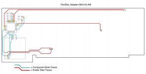
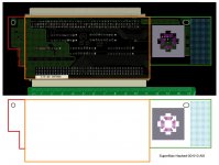
Spent a little time updating the layout of the board as best I can without someone contributing by taking pictures of the GAL IC from all sides to clarify more connections. So far I've identified a few inputs and one output to the adapted cache slot for the PowerCache. HELP! :ph34r:

TwinSlot_Adapter-000-010-2p.jpg

Oh yeah! Buzzing the connections would be invaluable.

 
Last edited by a moderator:
Trash80toHP_Mini

NIGHT STALKER
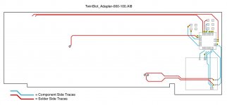
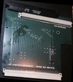
Mirrired to match up with Solder side

ARTMIX-DiiMO_Clone.10.jpg

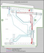
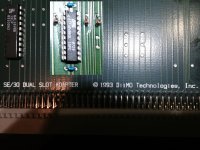
DiiMo card also mirrored. No Solder Side pic available as yet: DiiMO-SE30_Dual_Slot-10.jpg  .  .  .

DiiMO-SE30_Dual_Slot-10.jpg

ARTMIX Clone detail as compared to DiiMo Adapter: ARTMIX-DIIMO_GALs-Detail-20.jpg

ARTMIX-DIIMO_GALs-Detail-20.jpg

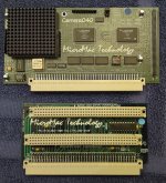
MicroMac version of DayStar TwinSlot Adapter/IIsi

MicroMac-Carrera040-Adpter.jpg

Mystery SE/30 Adapter for SE/30: Got info to contribute?

Mystery_SE30_Adapter.jpg

________________________________________________________________________

End game for project: One card adaptable to IIsi and SE/30 with these capabilities a/o Two NuBus slots in lieu of IIci Cache slot in IIsi (possibly two Nubus Slots for SE/30 in addition to IIci Cache Slot adaptation fot Universal PowerCache Accelerator.)for my Rocket 33 and Futura II FX/Video/10bT combo card. Dunno final specs are in flux.

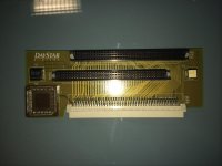
Daystar IIsi Adapter with PowerCache Slot, FPU and a NUBus slot! [:)] ]'>

View attachment 11540

All cards (except Mystery Card appear to this idiot to be variations on DayStar's TwinSlot Adapter for the IIsi with variations on the Adaptations by four different designers.

Playtime big time! [:D] ]'>

General Purpose PDS Prototyping Card for SE/30/IIsi, gotta be an open source project for some four layer PCB design Guru's input. One 74LS input limit electrical signal limitations require line drivers for signals to be added. Auxiliary PSU input required as well as airflow enhancement to meet/exceed existing power/cooling budgets of both target machines.

It's all been done, just gotta figure out how and tweak with SMT equivalents to the 74LS components of the day.

SuperMac-Hacked-00-010.jpg

68030 thruholes replace FPU socket provosion on 6030PDSGPPB for jumper wiring full signal set to SMT pads for 20pin/28pin GAL Activ Adaptation for two target machines. Addition of pin level 68030 PDS Socket provides for convenient form factor Slot interface to piFrastructure/shield level hacking.

 
Last edited by a moderator:
off

Member
Okay, so please don't hit me if I'm wrong here - but I have the following card and I'd be able to beep it out.
Would that help your efforts or is this the wrong one (it is working in my SE/30 so I might be completely wrong)?

IMG_0713.JPG


Trash80toHP_Mini

NIGHT STALKER
OMG!!!!!! That's the ONE!  [:D] ]'>  Yes, if you could buzz the connections from those two chips to wherever they go it would be a tremendous help! THX ever so much for joining the fray!

How can that card work in an SE/30? Do you have it installed in the PDS passthru of another card?

 
Last edited by a moderator:

off

Member
Glad to be of help! I'll try to buzz them asap, for the time being here are the images I shot over the years, maybe you can go ahead and lookup the chips to begin with: https://goo.gl/photos/Bdw1Sa4gCgm9jcF76

As for why this works in my SE/30: I honestly don't know - I acquired the card at about the same time as my Turbo but that was merely a coincidence (nevertheless a very happy one).

It works both, connected directly to the PDS slot in the SE/30 and through the Asante PDS-Passthrough.


Trash80toHP_Mini

NIGHT STALKER
How does it possibly fit into the SE/30 slot? Is the opening in your chassis much longer than usual so that you can plug it directly into the PDS? That CoPro socket section should interfere with the chassis?

edit: just checked your pics, I can't wait to throw them into my Illustrator file, it looks like exactly the same card layout I was working from in developing the pinout diagram! [:)] ]'>

 
Last edited by a moderator:

Trash80toHP_Mini

NIGHT STALKER
It is and I'm very pleased to hear it functions correctly in the SE/30.

Played a bit in Illustrator and the card's PCB seems identical the the one in the scans over in the NuBus Mafia collection on 'fritter. That's what I snagged as my template. I've now got off's pictures set up in layers in a new rev of my visual schematic. The only differences I can see are that the pads for the smaller 20pin IC and the CoPro Socket are populated.

I wonder if the card works fine in the IIsi with just the larger 28pin PAL(GAL?) on board? Maybe the SE/30 requires both? Dunno, we'll get it figured out eventually!

off, would you like to work from my Illustrator diagrams looking at the PCB from the solder side or the component side? I'll rough in the control pins/signals for all three slots. I'll keep Data, Addressing, Power, Ground etc. in invisible layers so you won't need to test quite so many possible connections. [:)] ]'>


off

Member
Yes, the illustrator file would be much appreciated!

If possible (don't have Illustrator at hand), I'd love something that either Sketch can edit (SVG?) or that I can print (read: PDF) and write on.

Regarding "does it fit the SE/30 case": Nope, it does not. Not without the Asante Ethernetcard anyways.

Even then, it's a very, very instable sandwich and honestly: If anything, this project would be the perfect solution to my problem (read: diy board with a layout that would better fit the SE/30).

I know the Stratos is out there - but why not do it yourself? ;)

As a final note, I was able to figure out what chips there are on the board: It seems both of them are PALs, the bigger one being a TI PAL20L8 and the smaller one being a TI PAL16L8.

Once the layout if figured out, I guess we can also figure out a way to dump these - from what I can see in the docs there is no memory and as such every programmed function can not rely on any internal state. Might be mistaken on that, but we can go into details later on. I should have everything at hand to make up a dumping tool, but that is for later as well :)


Trash80toHP_Mini

NIGHT STALKER
That's what I thought was going on physically with your card, had to be. Strange that there are versions floating about with either one or two PAL configurations. I'm off tomorrow, so I'll get more in on the AI8 file and I can always export it in .pdf for your markup.

It's funny you mentioning reading the PALs on your board. I'm assuming all have had their security fuses blown, so I'm in the beginning stages of setting up an Orange pi ONE to brute force all the possible I/O combinations out of each and every one of the little bat rastards I can lay my grubby little paws upon. So far I've got 'em for two other adapters I still need to depopulate and scan.

I fugure you'll be wanting to "see" the graphic from the component side. I usually look at 'em from the solder side, it's way faster to buzz the connections from that side, but heck to keep in contact with the source pin. If you've got rows of header pins it's probably easier to plug 'em into the connectors and buzz from the top. I'll give that a look see, I just got a bunch of long header/socket pairs in from China.

 
Top