• Updated 2023-07-12: Hello, Guest! Welcome back, and be sure to check out this follow-up post about our outage a week or so ago.

Early Macintosh home brew 4MB memory upgrade board development

Golden Potato

Active member
I just want to confirm, did you cut the traces to pins 12 and 13 of the TSM chip?.
No I did not. I see that they (~CAS0 annd ~CAS1) aren’t necessary to take back to the logic board and could instead be pulled up high. I’m not sure if it would be necessary because original memory should be disabled as their ~RAS line is pulled high. Maybe the DRAMs still respond somehow to ~CAS signal pulses even when ~RAS is unasserted?

I think the schematic should be changed to pull the ~CAS lines high as well just to be sure.

Thanks again for looking over and thinking about this!
 

Builder68

Active member
No I did not. I see that they (~CAS0 annd ~CAS1) aren’t necessary to take back to the logic board and could instead be pulled up high. I’m not sure if it would be necessary because original memory should be disabled as their ~RAS line is pulled high. Maybe the DRAMs still respond somehow to ~CAS signal pulses even when ~RAS is unasserted?

I think the schematic should be changed to pull the ~CAS lines high as well just to be sure.

Thanks again for looking over and thinking ab
 

Builder68

Active member
Absolutely, moving to a PCB layout sounds like the way to go!

On the topic of the ~CAS lines, pulling them high on the PCB can be very beneficial. It helps reduce noise. It also offers a slight power consumption reduction which is always a bonus.

This is incredibly exciting! Your progress on the RAM expansion board for the Macintosh 512k is truly groundbreaking. No one's attempted this in 30 years, and it's fantastic to see you pushing the boundaries. Please keep us updated on your progress – we're all eager to see how this unfolds!
 

Golden Potato

Active member
Adrian Black released a follow up video to the memory upgrade board on a Mac 512K logic board he was fixing up (I believe these are on his second channel). It got me thinking that bodge wires leading into a connector as a removal means for a memory upgrade mod isn’t such a bad way to go. Sure, it’s not as clean as pin headers into IC sockets, but it can be designed to no longer require desoldering custom Apple ICs.

With that in mind, I took another look at the Apple schematics and the logic board itself to come up with the following list for making connections to the logic board. It would also be a little easier for me to lay out the PCB since there will be fewer pin headers to accurately align with the logic board IC sockets.

Signal Logic Board Tap ------- --------------- RA0 RP2-1 RA0F RP2-2 RA1 RP2-10 RA1F RP2-9 RA2 RP2-5 RA2F RP2-6 RA3 RP2-7 RA3F RP2-8 RA4 RP2-4 RA4F RP2-3 RA5 RP3-1 RA5F RP3-2 RA6 RP3-5 RA6F RP3-6 RA7 RP3-3 RA7F RP3-4 ~CAS0 RP3-8 ~CAS0F RP3-7 ~CAS1 RP3-10 ~CAS1F RP3-9 +5V U12E-20, U13E-20 GND U12E-10, U13E-10 D0 U12E-18 D1 U12E-16 D2 U12E-14 D3 U12E-12 D4 U12E-3 D5 U12E-5 D6 U12E-7 D7 U12E-9 RQ0 U12E-2 RQ1 U12E-4 RQ2 U12E-6 RQ3 U12E-8 RQ4 U12E-17 RQ5 U12E-15 RQ6 U12E-13 RQ7 U12E-11 D8 U13E-18 D9 U13E-16 D10 U13E-14 D11 U13E-12 D12 U13E-3 D13 U13E-5 D14 U13E-7 D15 U13E-9 RQ8 U13E-2 RQ9 U13E-4 RQ10 U13E-6 RQ11 U13E-8 RQ12 U13E-17 RQ13 U13E-15 RQ14 U13E-13 RQ15 U13E-11 RA8 WIRE TO R42-(SIDE CONNECTED TO U13G-7) RAM-R/~W WIRE TO R33-(SIDE CONNECTED TO U2E-13) ~RAS WIRE TO R4-(SIDE CONNECTED TO U1D-14) C2M WIRE TO VIA WHICH CONNECTS TO U4G-14 VID/~u WIRE TO VIA BELOW U1F A19 WIRE TO RP1-7(PIN 2 IN SCHEMATIC) A20 WIRE TO R28 (SIDE CONNECTED TO U4D-5) A21 WIRE TO VIA WHICH CONNECTS TO U2D-9

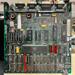
The attached photo has red highlights where two SIP resistor packs and two tristate buffer ICs would need to be desoldered and replaced with female machined pin headers/sockets. The magenta highlights indicate connections for wires which will lead to a connector to plug into the upgrade board.
 

Attachments

  • IMG_4999.jpeg
    IMG_4999.jpeg
    1.3 MB · Views: 14

Golden Potato

Active member
A feature that the memory expansion board Adrian found on that 512K logic board was that you could hold the mouse button down at power on (like you would do to make the system eject a disk) to have the memory board disable itself leaving the system with only 512K of memory. System reset reenables the upgrade board unless the mouse button is held.

I’m not sure if there’s some software that can’t handle the additional RAM? I’m not sure why else this feature would exist. If anyone can think of a good reason for it, I don’t think it would be very difficult to implement.

I’ll probably start thinking about SCSI as well. I wasn’t originally going to look into that because I already have a SCSI add on card, and it uses a custom IC or two in addition to the SCSI controller IC to make it work. I wasn’t sure if there was something tricky going on with those custom ICs, but I’m beginning to think they were just for address decoding.

If implementing SCSI really only requires adding a SCSI controller IC (with termination resistors and also a diode to provide termination power for BlueSCSI boards) and slap together some address decoding logic placing it into the correct place in the memory map, then I bet it wouldn’t be that hard to do. I haven’t done much research on this yet, so that may be a false sense of self confidence.
 

Golden Potato

Active member
I found this build thread for reverse engineering a MacSnap SCSI card. It uses some clever, slightly complicated, hacks to make it work using only the lines available at the ROM sockets, but I don’t think that’s necessary if we are already soldering leads to various points on the logic board.

Great information here, especially the tip about the system checking if it’s a Mac Plus by looking for ROM mirrors. While the MacSnap board solved this in software via a hacky on-the-fly patch, I think it could be solved in hardware with additional address decoding logic.


Builder68

Active member
Adrian Black released a follow up video to the memory upgrade board on a Mac 512K logic board he was fixing up (I believe these are on his second channel). It got me thinking that bodge wires leading into a connector as a removal means for a memory upgrade mod isn’t such a bad way to go. Sure, it’s not as clean as pin headers into IC sockets, but it can be designed to no longer require desoldering custom Apple ICs.

With that in mind, I took another look at the Apple schematics and the logic board itself to come up with the following list for making connections to the logic board. It would also be a little easier for me to lay out the PCB since there will be fewer pin headers to accurately align with the logic board IC sockets.

Signal Logic Board Tap ------- --------------- RA0 RP2-1 RA0F RP2-2 RA1 RP2-10 RA1F RP2-9 RA2 RP2-5 RA2F RP2-6 RA3 RP2-7 RA3F RP2-8 RA4 RP2-4 RA4F RP2-3 RA5 RP3-1 RA5F RP3-2 RA6 RP3-5 RA6F RP3-6 RA7 RP3-3 RA7F RP3-4 ~CAS0 RP3-8 ~CAS0F RP3-7 ~CAS1 RP3-10 ~CAS1F RP3-9 +5V U12E-20, U13E-20 GND U12E-10, U13E-10 D0 U12E-18 D1 U12E-16 D2 U12E-14 D3 U12E-12 D4 U12E-3 D5 U12E-5 D6 U12E-7 D7 U12E-9 RQ0 U12E-2 RQ1 U12E-4 RQ2 U12E-6 RQ3 U12E-8 RQ4 U12E-17 RQ5 U12E-15 RQ6 U12E-13 RQ7 U12E-11 D8 U13E-18 D9 U13E-16 D10 U13E-14 D11 U13E-12 D12 U13E-3 D13 U13E-5 D14 U13E-7 D15 U13E-9 RQ8 U13E-2 RQ9 U13E-4 RQ10 U13E-6 RQ11 U13E-8 RQ12 U13E-17 RQ13 U13E-15 RQ14 U13E-13 RQ15 U13E-11 RA8 WIRE TO R42-(SIDE CONNECTED TO U13G-7) RAM-R/~W WIRE TO R33-(SIDE CONNECTED TO U2E-13) ~RAS WIRE TO R4-(SIDE CONNECTED TO U1D-14) C2M WIRE TO VIA WHICH CONNECTS TO U4G-14 VID/~u WIRE TO VIA BELOW U1F A19 WIRE TO RP1-7(PIN 2 IN SCHEMATIC) A20 WIRE TO R28 (SIDE CONNECTED TO U4D-5) A21 WIRE TO VIA WHICH CONNECTS TO U2D-9

The attached photo has red highlights where two SIP resistor packs and two tristate buffer ICs would need to be desoldered and replaced with female machined pin headers/sockets. The magenta highlights indicate connections for wires which will lead to a connector to plug into the upgrade board.

Last night I also watched latest Adrian's video (Very well done, funny and entertaining, by the way, as are his videos usually). I couldn't agree more with you about the way of making the connections to the motherboard (which by the way would be a considerable improvement over the initial approach; this way of making the connections is the best I've seen among all the commercial expansions). On the other hand, the implementation of the mouse button seems to be entirely hardware-based, and at first glance, the logic needed to do it seems straightforward. Perhaps the mouse button signal identified in the video by Adrian pulls high (deactivate) the additional CAS lines for the memory expansion, and then resets the CAS lines for the onboard memory to resume normal operation. Then the ROM handles the rest reallocating the memory space accordingly.

By the way, I noticed the screen pattern during the Mac's memory test is very similar to your earlier video. It seems your breadboard design works intermittently, possibly due to interference. This suggests your design functions, but noise inherent to breadboards might be the cause of the unexpected results.
 

Builder68

Active member
I got curious. Are there any reasons why the bigger 1MB x 16-bit CMOS FAST PAGE RAM ICs, like the ones in some Mac Classic/SE memory upgrades, wouldn't work in the early macs?

The reason I ask is because those teeny 1Mbit x 4-bit chips you used in the prototype seem like a pain to find these days. I stumbled on the AS4C1M16(F/E)5 as a possible swap – seems compatible, and just two would hit 4MB. Maybe just a small modification on the CAS generation of your design would be all it takes? Or is there something in the logic that wouldn't play nice with these bigger chips due to the 16 bit bus registration at once?

Thanks!
 

Builder68

Active member
I'm also considering the KM44C4100 (4Mb x 4bit), in order to keep the CAS generation unmodified.


Attachments

  • KM44C4000C.PDF
    347.9 KB · Views: 3

Golden Potato

Active member
I got curious. Are there any reasons why the bigger 1MB x 16-bit CMOS FAST PAGE RAM ICs, like the ones in some Mac Classic/SE memory upgrades, wouldn't work in the early macs?

The reason I ask is because those teeny 1Mbit x 4-bit chips you used in the prototype seem like a pain to find these days. I stumbled on the AS4C1M16(F/E)5 as a possible swap – seems compatible, and just two would hit 4MB. Maybe just a small modification on the CAS generation of your design would be all it takes? Or is there something in the logic that wouldn't play nice with these bigger chips due to the 16 bit bus registration at once?

Thanks!
I’m pretty sure I bought mine on eBay. I don’t reallly remember my reasoning for settling on that part other than the low price.

I appreciate you searching for parts which are easier to obtain! This 1Mx16-bit (2MB?) chip you linked looks like it should work great, since it has separate lower and upper byte column address strobes (~LCAS and ~UCAS). That’s essentially what ~CAS0 and ~CAS1 are.

So it’s like two 1Mbyte 8-bit chips in one package. I think you’re correct in saying two of these would equate to 4MB. They have the right number of address inputs (A0-A9) and the entire circuit would need four ~CAS lines, and that all matches up with my proposed design!

I’ll use this part when I update the schematic with new connections to the logic board.
 

Golden Potato

Active member
I'm also considering the KM44C4100 (4Mb x 4bit), in order to keep the CAS generation unmodified.
We would need to use four of these 4Mb chips just to have the correct number of data bits, and I think it would end up providing 8MB of memory, half of it being wasted unless we tried to do something tricky and find some extra address space for a RAM disk? I don’t know much about that nor the software required to make it work.

The system’s ~CAS0 and ~CAS1 could be used directly. Instead of generating more ~CAS lines to accommodate the additional address space, we would just need to generate one more RAM address line (RA10) beyond the one we were already making (RA9). We would need to use the 2K refresh version of the chip to make sure the column and row addressing remained consistent: A0-A10 for both and not A0-A11 & A0-A9.

Thinking about it further, and I’m racking my brain trying to figure out how we would generate RA10 using the 74LS253 approach. That was done on the Mac 512K in pairs, for example to create RA8: A17 or A18 is sent to the RAM chips depending on the state of C2M. The pair A19 and A20 are to be used to create RA9. I’m not sure what we would do with just A21 to create RA10.

Probably better off sticking with the approach that creates four ~CAS lines. That’s similar to the way the Mac Plus does it.
 

Builder68

Active member
We would need to use four of these 4Mb chips just to have the correct number of data bits, and I think it would end up providing 8MB of memory, half of it being wasted unless we tried to do something tricky and find some extra address space for a RAM disk? I don’t know much about that nor the software required to make it work.

The system’s ~CAS0 and ~CAS1 could be used directly. Instead of generating more ~CAS lines to accommodate the additional address space, we would just need to generate one more RAM address line (RA10) beyond the one we were already making (RA9). We would need to use the 2K refresh version of the chip to make sure the column and row addressing remained consistent: A0-A10 for both and not A0-A11 & A0-A9.

Thinking about it further, and I’m racking my brain trying to figure out how we would generate RA10 using the 74LS253 approach. That was done on the Mac 512K in pairs, for example to create RA8: A17 or A18 is sent to the RAM chips depending on the state of C2M. The pair A19 and A20 are to be used to create RA9. I’m not sure what we would do with just A21 to create RA10.

Probably better off sticking with the approach that creates four ~CAS lines. That’s similar to the way the Mac Plus does it.
You're absolutely right about the refresh rates! I completely missed that aspect. Regardless, your explanation was incredibly helpful and provided a much clearer, broader understanding of how RAM functions in the early Macs.
 

Golden Potato

Active member
You're absolutely right about the refresh rates! I completely missed that aspect. Regardless, your explanation was incredibly helpful and provided a much clearer, broader understanding of how RAM functions in the early Macs.
What I meant in the part about refresh rates was more about the address lines than actual rates. I was originally confused about that chip having an A11 pin, because A10 should be the MSB for that size of memory chip. Then I noticed the little blurb in the datasheet block diagram regarding the address signals. I don’t really understand how one would implement the 4K refresh type with the strange address line usage, but I guess that doesn’t really matter for this project.

I’ll admit I haven’t looked into the timing aspect of any of this yet. I’m just crossing my fingers that I’m not adding too much propagation delay and it’ll just work. Hopefully faster memory will make up for it? If it doesn’t work out, and I can always poke around with the scope and see what we can see.

I’m sort of figuring this out on the fly, so don’t take any perceived confidence on my end as credibility 😆 This has very much been a learning opportunity for me. In this thread, I’m mostly thinking out loud hoping others will catch any misunderstandings I may have. However it is not my intention to spread misinformation if I am thinking about any of this incorrectly.
Back in college, it was a pretty common occurrence for me to confidently convince everyone else in my group to believe or think a certain way, just for me to eventually realize I misunderstood something and had to backtrack. So sorry if there’s some whiplash, and I end up going in a different direction.

I really appreciate the dialog. This is the sort of thing I was hoping for when posting.

By the way, I’ll try to hone in on redrawing the schematics soon and spend less energy on scope creep for now. We can always circle back to fancy mouse click memory upgrade disabling and SCSI stuff in the future.
 

Golden Potato

Active member
I got curious. Are there any reasons why the bigger 1MB x 16-bit CMOS FAST PAGE RAM ICs, like the ones in some Mac Classic/SE memory upgrades, wouldn't work in the early macs?

The reason I ask is because those teeny 1Mbit x 4-bit chips you used in the prototype seem like a pain to find these days. I stumbled on the AS4C1M16(F/E)5 as a possible swap – seems compatible, and just two would hit 4MB. Maybe just a small modification on the CAS generation of your design would be all it takes? Or is there something in the logic that wouldn't play nice with these bigger chips due to the 16 bit bus registration at once?

Thanks!
I’m having a hard time finding where these can be purchased. I found an alternative on Mouser, but it’s 3.3V only and the inputs are not 5V tolerant. A couple of level shifters would solve that issue. We would still need a 3.3V power supply.

Unless you can point me to some readily available 5V versions, for now I’ll stick with the memory ICs I have on hand. I’m thinking a future revision should use 3.3V ICs and converters.
 

Builder68

Active member
I’m having a hard time finding where these can be purchased. I found an alternative on Mouser, but it’s 3.3V only and the inputs are not 5V tolerant. A couple of level shifters would solve that issue. We would still need a 3.3V power supply.

Unless you can point me to some readily available 5V versions, for now I’ll stick with the memory ICs I have on hand. I’m thinking a future revision should use 3.3V ICs and converters.
Hey, those ICs can be found on Aliexpress, Amazon or EBay! (By the way, I snagged a couple already to play around with your design as soon the arrived.). It looks like there is a large stock available (brand new) at several main suppliers.
 
Last edited:

Builder68

Active member
FYI, those ICs are also used in the 3MB RAM expansion board for the Macintosh Classic (Made by Garrett's Workshop)

The design (Kicad) files are available at GitHub .

That's interesting that this board is only 3 years old! It makes me think the designers faced a similar challenge to what you have now - finding compatible RAM ICs for these compact Macs. Seeing this IC work with the Classic is a great sign! Since the Classic is very similar to the 512k, this bodes well for your project, don't you think? 😉
 

Golden Potato

Active member
FYI, those ICs are also used in the 3MB RAM expansion board for the Macintosh Classic (Made by Garrett's Workshop)

The design (Kicad) files are available at GitHub .

That's interesting that this board is only 3 years old! It makes me think the designers faced a similar challenge to what you have now - finding compatible RAM ICs for these compact Macs. Seeing this IC work with the Classic is a great sign! Since the Classic is very similar to the 512k, this bodes well for your project, don't you think? 😉
Agreed, that’s a great sign that it should work for this project!

Thanks for sharing this. I saw a blurb in the schematic in the linked GitHub repository talking about using an AND gate to control the ~OE line to the RAM ICs based on either the upper or lower ~CAS lines being asserted rather than just tying ~OE low like I had originally. The purpose for this allowing the use of EDO type RAM if FPM type becomes unavailable.

One more criterion to add to the list for the schematic redraw!
 
Top