• Updated 2023-07-12: Hello, Guest! Welcome back, and be sure to check out this follow-up post about our outage a week or so ago.

Apple /// restoration

pball52998

Well-known member
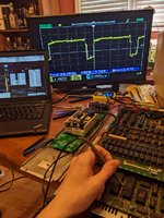
Guess who has a new osciliscope that can pick up MHz, replaced a crystal and now gets 14.3mhz on pin 5 B13.

This guy! Wooo!

1670716443895.png

Off to find the rest of the brokenness in this machine.. pin 5 matches basically what 6 and 8 see for output (expected 14.3mhz)

Pin 12 is sending out 7mhz, good
1670717028871.png
Pin 13 has 3.5mhz, good
1670717065697.png

I'm just ecstatic to see life here.

Pin 37 however of the 6502. Not looking so hot.
1670717215556.png

Don't think it's supposed to look like that..

Continuing on with B13 -> B12.

Pin 2 - 7mhz - good
Pin 3 - 7mhz - good
Pin 4 - 7mhz - good
Pin 5 -> entry point from B13 -> 7mhz -> Good
Pin 6 - 3.5mhz - good
Pin 7 - 3.5mhz - good
No pin 8 in logic diagram
Pin 9 - 14mhz - good
Pin 10 - 1mhz - uhhh, ???? -
1670718745795.png
Pin 11 - 1mhz - uhh, ???? Looks like it's not happy
1670718624804.png

Those looks off, supposed to be a 1mhz clock signal if I read correctly.
1670719284324.png

Anyone else looking at the schematics:

Know if that's expected or where a 1mhz clock signal would come off?

I decided to take another look at the video logic again.

Seems it "starts" with D4? Right?


Both show C1m, the 1mhz clock signal?

I get a 60hz wave there (expected..?)

Ignore pin 10 and 11 of B12? Or seems wrong?

Sorry for the long post. Just excited to SEE something! No video yet of course lol, but we're getting somewhere
 
Last edited:

pball52998

Well-known member
Went down a small rabbit hole on this one too.


1670727327330.png

If I'm reading this correctly, the logic prom is sending a signal to D5 -> E7 -> A11 -> PH0 which is the input on the 6502

Starting from the F7 pin 13 PROM:

1670727558221.png

This carries exactly to E7 pin 8.

Then the moment it reaches A11 pin 2 it turns into this garbage.
1670727732288.png

This carries out of pin 5 directly into PH0, input on the 6502. Which sees exactly what's coming in on pins 2.

Possibilities of A11 being bad? One of the only IC not socketed unfortunately.

Or something along the path?

Interested to hear any ideas on that one, along with getting CPU fixed before video? Or try to bum rush getting video fixed?

If video, is it separate from the CPU like the ii? I imagine so.

Trying to look at video logic since I've gotten a small piece of the timing figured out (so happy about that!)


Work forwards? Or backwards?

If working backwards

Using NTSC b&w video it seems L8 and H3 are the final spots.

But thinking logically for me and questions from me.

Where does a video signal start? When do we actually start to see NTSC and it's possible to pick up with a osciliscope I imagine.

Start with the PROM? Or with some of the other chips? Line E/F/G?

Can I trace the video signal down the path / from the start like I am doing the signals to the CPU?

Sorry for the triple post. Just excited to continue with some more proper tools!
 

mdeverhart

Well-known member
This carries exactly to E7 pin 8.

Then the moment it reaches A11 pin 2 it turns into this garbage.
Possibilities of A11 being bad? One of the only IC not socketed unfortunately.
If it’s good at the output of E7 and bad at A11, it’s more than likely a disconnect in the signal somewhere along the way. If E7 is socketed, then the pin of E7 might not be making contact with E7’s socket. I’d measure E7.8 at both the IC pin and at the socket pin where the socket is soldered to the board.

If it’s good at the socket pin, then it could be a broken trace or solder issue somewhere between E7 and A11. If A7 were bad and it was dragging down the signal you’d see the same thing at E7.8 - which is why it’s more likely that there’s a disconnect somewhere along the line.
 

pball52998

Well-known member
If it’s good at the output of E7 and bad at A11, it’s more than likely a disconnect in the signal somewhere along the way. If E7 is socketed, then the pin of E7 might not be making contact with E7’s socket. I’d measure E7.8 at both the IC pin and at the socket pin where the socket is soldered to the board.
I think my ground might have been messed up to be honest. Too tired + trying to properly do things I guess doesn't go well.

So ignore my troubleshooting in post #123. I am so sorry folks. Silly mistakes intensify.. I knew 60hz waves didn't look right. Especially such large ones. Darn auto function. I've dialed in numbers of where all the different mhz are for now.

So going to try and look at it more this morning in a fresh mind state. Kept waking up last night thinking about what I did wrong.

So I'm looking at this diagram yet again. Timing seems to be a pain!

1670763163167.png

I decided to go even further back. F7, pin 5, C1m, has to come from somewhere.

It leaves B12 on pins 10 and 11 perfectly at 1.19mhz.

I know it leaves B12, because D11 in this diagram sees 1.19mhz come in on pin 2 -> leave pin 5 or vice versa, in pin 5 out pin 2. (it's right above it, cut off in the screenshot)

So I checked the bottom of the board where pin 5 is for F7. 1.19mhz, yay! So that works.

Checks leg..dead as a doornail. Nothing coming in.

Cleaned the socket and chip again and finally a 1.19mhz singal is there.

Pin 13 now sending 1.19 -> D5 12 -> D5 9 empty. Swapped D5 and D11, still nothing on D5 pin 9.

D05 is a 74S74
1670766799926.png
1670766747606.png
Could it be something with E7 stopping the flow to pin 9?

E7 is looking for Q0 and RAS. Q0 comes from D10 pin 15 carrying a 1.79mhz.

E7 pin 12 just sees flatline unfortunately.

RAS comes from B12 pin 14 and looks like a nightmare.. don't know what it's supposed to really see.

Going to stare at these schematics again to see if I can make sense of it.

Head scratcher for the day I guess is trying to look at timing.
 

mdeverhart

Well-known member
D5 is a D-flip flop, rather than a logic gate, so it behaves a bit differently. A rising edge on the CLK input causes the value on the D input to be latched and driven on the output Q. The trick is that the value of Q stays the same even if D changes, until there’s another rising edge on the CLK input.

The exceptions are the CLR (clear) and PRE (preset) inputs, which set the flip-flop (and D output) to 0 (CLR) or 1 (PRE) immediately, regardless of the CLK input.

So - until you see a rising edge on the CLK input (driven by the output E7.11), you won’t see any change on the output D5.9
 

pball52998

Well-known member
So - until you see a rising edge on the CLK input (driven by the output E7.11), you won’t see any change on the output D5.9
Nice to know I was reading that correctly then!

Thank you for the explanation.

E7 is a simple 74LS001670772241665.png
So 12 and 13. Reseated and cleaned the socket again.. and...

Guess who has a 2mhz clock signal!
1670772608537.png

The 6502! WOO!
 

pball52998

Well-known member
Hooray! I can’t believe these sockets are so bad.
I keep thinking I'm crazy, but I clean the IC and socket again, sand legs again and bam clock on the CPU.

Amazing how dirty this board was!

Trying to track down where the hell my video is though!

I understood the timing logic diagram after staring at it for a long time a bit more, looking up the IC layouts. etc.

For anyone wondering, and scope may be off a bit, but seems close enough to what it's supposed to be. Every data line:

1670777422085.png

Address lines seem a wee jumpy..

1670777867638.png

Most look like this, not sure if scope is just acting odd with that signal or if the address line is actually screwy.

Anyone know of a good jumping point to start with video? I look at the video diagram and get kinda startled.


Just happy to be making solid progress now it seems

Edit to this: curse the person who made the memory board go on top of where most the video logic is. Like why. Please. Why.
 

mdeverhart

Well-known member
Address lines seem a wee jumpy..
I wouldn’t worry about that (for now, at least). I think most of what you’re seeing is scope persistence and multiple triggers - the patterns on address/data lines won’t be periodic like clock signals. Clock signals will display (mostly) clean on the scope, because they’re constant at the same frequency and voltage levels (more or less). For non-periodic signals you’ll see overlapping captures depending on how the scope is configured. With persistence and auto-triggering you’ll see overlapping traces like that. If you were to set the scope for single triggering you’d just get one trace.

For the address/data lines, I’d focus on making sure they’re toggling (not stuck low/high), and that they’re fully connected between each driver and receiver. (Or that they’re toggling at each connected component, ideally at the IC leg since you’re dealing with dirty sockets).
 

pball52998

Well-known member
For non-periodic signals you’ll see overlapping captures depending on how the scope is configured. With persistence and auto-triggering you’ll see overlapping traces like that. If you were to set the scope for single triggering you’d just get one trace.
I set it to trigger mode normal and stopped during capture and it looks a lot more like what I'd "expect" to see? If that's what you're referring to at least.

Data: edit: accidentall used wrong photo, inserting correct one, no different but is a stopped capture.
1670779766773.png


Address:
1670779354597.png
 

Attachments

  • 1670779270014.png
    1670779270014.png
    776.5 KB · Views: 6
Last edited:

mdeverhart

Well-known member
Yep, that’s it! The waveforms will depend on the access pattern, but that should be good enough to make sure they’re getting to the memories, video circuit, etc.
 

pball52998

Well-known member
Moved on to the next part of the logic diagram.
1670787045168.png

After cleaning, swapping, checking, IC checker etc I can confirm one of these IC is dead. G12 74LS161.

Moved it, cleaned it, checked underside and everything is good. No matter where I put it, it stays no signal on what is now G12 C1M pin 2.

So on the "buy list" so far is a:
G12: 74LS161
Keyboard encoder from JCM since mine literally fell to ash, god bless this retro community.

So I guess a question, till I get that "fixed" (being G12) how much farther can I troubleshoot since that is part of the timing logic?

It feeds V2-5 which go to F8 in turn going to G9 which is a ROM.

Guess what that rom is... 341-0030 Video elements/attributes generator. lol

Seems without that I can't even get to start video troubleshooting till I get that fixed I guess.

F8 also feeds G10 -> J8 which feeds display.

Looks like I gotta fix G12 first.

Anything in the meantime? I'll see how the other pins are re-acting / feeding to the ROM at least, that seems logical.
 

pball52998

Well-known member
New on the list of things that just screwed up.

A resistor that blew out.

Put G12 back in, turn on to look at something.

1670788139127.png

Hear a pop/crack and a burning smell. Turn it off and look by smell and bam, a resistor that went boom.

That'll be getting replaced.. in the meantime. Anyway to know what could've caused it? It's R43. I can try and find it in one of the schematic pages but might not be able to directly understand why.

I tried to trace it on the board but god those traces are tiny and go under IC and such

Not going to turn it back on till I get another resistor and new IC at least though.

Unless it's safe to, but I assume not since those usually blowing is definitely not a good sign
 
Last edited:

joshc

Well-known member
Some of those traces look scabby (see the black marks along the traces), do they have continuity?

Some of the solder joints look pretty scabby too, can you try to clean them up a bit more?
 

pball52998

Well-known member
Well, in an unexpected place.

Keyboard logic!

https://apple3.org/Documents/Schematics/Keyboard Logic.jpg

1670791936289.png
APPLE /// LOGIC SIGNAL SOURCE

Signal Location Meaning
KVCC 9-4b KEYBOARD VCC

1670792198930.png

1670792218433.png

From the manual
Keyboard Light: The keyboard light indicates the VCC is provided to the keyboard. If no light is observed, check Q9 [MPV 511]

So the power to the keyboard (not plugged in) caused the resistor to blow from the transistor?

I don't even have the keyboard IC plugged in since it basically turned to ash (rusted entirely and over 12 legs fell off just taking it out), nor the cable for the keyboard.

Don't think the connector to the keyboard needs to be plugged in to test.. but I may be wrong!

Again sorry the repeated messages.

Hope someone can come across this thread 20 years in the future and appreciate the trouble I'm going through and find a answer some some random part I struggled with. lol

Wanting to log everything for anyone who ever has the same thing in the future. As /// information is well.. sparse compared to the ii.

Thankfully there's the manuals and schematics, just not the cleanest.
 

Attachments

  • 1670792493644.png
    1670792493644.png
    32.1 KB · Views: 3

pball52998

Well-known member
Some of those traces look scabby (see the black marks along the traces), do they have continuity?

Some of the solder joints look pretty scabby too, can you try to clean them up a bit more?
Most things that look like that have continuity from what I've tested (bottom of the board where I've been focusing)

I tested a couple of the traces that are right next to each other on the top of the board (where it was in the absolute worst condition, rust and everything) and some of them are absolutely dead. Specifically ones with solder joints that look terrible. Of course solder joints look terrible just not sure how much I trust that. Also dirty. Need to touch up an absolute ton of joints! I haven't touched up any of them besides what I've desoldered to check with transistors.

I think this whole board needs more than a light alcohol bath that I've already given it.

I'll probably take every IC out and clean with soap and water. Surprised I haven't done it yet.

Especially because now I have the first half of timing working..but it needs a deep clean.

Do people prefer soap and water cleaning through and through?

Or a nice 91% alcohol bath?
 
Top