• Hello MLAers! We've re-enabled auto-approval for accounts. If you are still waiting on account approval, please check this thread for more information.

Three Slot Riser for 6400 - In search of the Mythical Slot C

On the Tanzania tangent: @Daniël interesting block diagram, the monitor sticks out like a sore thumb, don't recall ever seeing that in any other DevNote? Makes me wonder if they were thinking about an inexpensive, industry standardized AIO for the K-12 education market? Housing a full blown PC/Windows setup on the order of the IBM PS/2 Model 25 might be interesting?

That Riser pic is interesting, looks to be capped off, limiting it to maybe four instead of the five slot option in the DevNote?
 
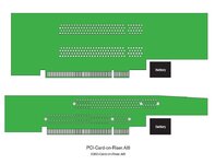
Back on topic: Roughed in the available real estate for 6x00, 5x00, 6360 for implementing your PCI card on a riser @Daniël
Haven't looked at the TAM riser yet, but it will be an amalgam of the two. An overlay of all three outlines will be interesting. The polygonal venn diagram would reveal the sweet spot of implementing the likes of SATA on risers fitting all four case form factors.

Battery position/size is approximate, but it could easily be moved over for clearance to increase available board area.
PCI-Card-0nRiser.jpg

Forgot what a CD deprived, hunchbacked, bare metal HarnessMonster mess I made of the 6360 to fit a 12" VidCard back in the day. So that deep 6360 TriSlot riser from yesterday was just silly, but it made a great start for today's design study. 🙂
 
Last edited:
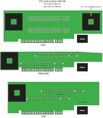
Done with this design study, looks to be room to implement a PCI Card on even my 6360/5x00 TwinSlot Riser. Gonna make those boards for my 6360 and the TAM eventually, those fit into the 10x10 SEEED square. Might as well break PCI out onto a PGA prototyping connector on a large board revision at some point?

PGA -Prototyping-Connectors-PCI-Card-on-Rise-Alchemy-Gazelle.jpg
Single slot RA Riser should be in soon for connection buzzing setup. Tired of AI playtime for a while I think.
 
Last edited:
Tested the 6360/5x00 and 6x00 riser mockups. Laser printed at work, spraymented to cardboard and just finished cutting them out and fitting them into the slots. They work great! Batteries can be scootched over a bit on their Velcro pads to clear the boards so more real estate is available on the riser cutoutss. No TAM available, but think it will work out fine as well.

Not sure we need extra space though. Forgot to mention that the PGA socket/PCI breakout connector is for mounting a prototyping daughtercard running in between the riser and CSII Card. On the 6360/5x00 there's about 5x the footprint of the PGA socket running alongside the riser. No need to do risers with electronics on them after all?

Definitely knocking this stuff off, single slot riser was in the mailbox, so I've got a nice stable platform to buzz connections on the 6x00 riser! :D
 
Last edited:
Could someone save the PCI/CSII page from the schematic and post that single page PDF. Want to get that page for opening it up in Illustrator 8 under 9.2.2.

TIA,
jt
 
Got the above figured out, it's in AI8.

I've got a great start on buzzing the 6x00 riser. Have to recheck my findings, but it looks like nine signals only make it up to Slot A from the motherboard connector. B18 in the PCI spec is +5V, my mistake in translations or another hijacked line on the Logic Board connector?
 

Attachments

Yep, got that one straightened out and a couple of others.

I'd mirrored the A signals to B, so same top and bottom as the error in that diagram, OOPSIE! :oops:

DELTA layer is coming together. I think I almost have the buzzing done and checked. Looks to be only two signals that differentiate Slots A&B? I'll post a .PDF of the mess, maybe tomorrow. ;)


edit: never mind, here's what I have. REQUEST and GRANT for Slot B are connected to RESERVED lines on the Logic Board Connector. Orang-ish lines appear to come to a dead end at Slot_A?
 

Attachments

Last edited:
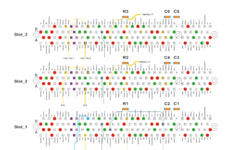
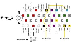
OK, I've got six questions for you. I scoured your messages and did the best I could to translate that into images betwixt my ears. This is what I came up with.:

I was thinking of Slot_A on the riser as Slot_1, but it appears to be Slot_0 from my read of the info you've related, what I can figure out from the schematic (not something I can easily wrap my head around) and my buzzing of the 6x00 Riser.

It looks like it might be possible to implement four slots and CommSlot_II as well?

If you can fill in the blanks for the six question marks on my AI doodle, we may be in business?

@trag how does this thing look to you?


edit: the ___? for Slot_3 REQUEST went astray, that'd be the sixth one, five are shown.
 

Attachments

Screenshot_20240904_084206.png
I think that should be it.
Not sure what you're doing with B23, that's Address 27 and should be a straight through connection.

As for "Slot 3", which I would assume you're wanting to be Slot E (CSII), you'd have to run wires like I did for Slot C on the Gazelle board, from the 74F32 IC (U23 on Alchemy, U20 on Gazelle).
You can get both REQ and GNT for CSII there, so if you wire it up to Slot 3's REQ and GNT, and set IDSEL to AD17, you'd get Slot E.

Which again, makes sense, if you consider the Slot Numbering on Alchemy and Gazelle:

AD13 -> Slot A (PCI Slot)
AD14 -> Slot B (PCI Slot)
AD15 -> Slot C (PCI Slot, Alchemy only)
AD16 -> Slot D (O'Hare)
AD17 -> Slot E (CSII Slot)
AD18 -> Slot F (ATi Rage IIc, Gazelle only)
 
OOPSIE! wrote this last night and didn't hit post:

Took another look late tonight and my brain hurts.
1 - Thinking above that Slot_A on the riser must be Slot_0 with 0-3 possible appears to have been cerebral flatulence? :oops:
2 - Buzzing the 6x00 Riser again just now was interesting:
- - - Reserved at A9 connects to Interrupt_C at A7 on the top slot (Slot_B/Slot_2)
- - - Interrupt_C at A7 is a straight thru connection to A7 of bottom slot (Slot_A/Slot_1)

_____________________________________________________________________________________________

Interesting stuff, got confuzzled again. Looks like you've narrowed the diagram down. Did you leave out what was labeled Slot_0 for clarity's sake?

Slot_1 above is the upper Slot of the standard, two Slot Riser with DELTA for:
INT Device select
Request
Yellow Grant line in your abbreviated adaptation is wired to A14 Reserved

B23 is Request and discovered it's a straight thru connection to both slots on the standard riser. Biggest surprise was that there is an IRQ anomaly on the stock riser that doesn't make sense at all.

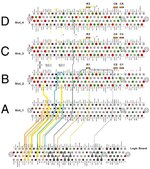
Alchemy-QuadSlot-001-DELTAX.jpg

Interrupt C bypasses Slot A and is connected to Slot B! If all interrupt lines are tied together on the Logic Board, what difference would that make? Most confusing, the others come to an abrupt halt at Slot A.

I have the three Reserved Lines (pink Contacts) left for connections to Grant and Request on the Mythical Slot C. That leaves what I thought might be D hanging in the breeze. It could likely be implemented with Jumpers from CSII, but that's probably silly. androda developed and is selling new design 10/100bT NICs for CSII. Gigabit NIC in PCI on Alchemy/Gazelle would likely only make a marginal improvement, so I'm leaving CSII untouched IRL, but will be experimenting with it for shiggles and gits.


New Project in the TwinSlot Riser project! If w unearth the Mythical Slot C, it looks like I can design a TriSlot Riser that'll fit the 6x00 drawer!
 

Attachments

Last edited:
I don't get these at all!
As for "Slot 3", which I would assume you're wanting to be Slot E (CSII), you'd have to run wires like I did for Slot C on the Gazelle board, from the 74F32 IC (U23 on Alchemy, U20 on Gazelle).
Do signals from those ICs make their way to pins (assuming "Reserved") on the Logic Boards Slot on either machine?

You can get both REQ and GNT for CSII there, so if you wire it up to Slot 3's REQ and GNT, and set IDSEL to AD17, you'd get Slot E.
It's looking like Slot_D would have to be jumpered from CSII. Lets hope the remaining three pin reserve of RESERVED lines will suffice to implement Slot_C in its own right as on the UMAX Riser. 🤞
 
AD13 -> Slot A (PCI Slot)
AD14 -> Slot B (PCI Slot)
AD15 -> Slot C (PCI Slot, Alchemy only)
AD16 -> Slot D (O'Hare)
AD17 -> Slot E (CSII Slot)
AD18 -> Slot F (ATi Rage IIc, Gazelle only)
You should be able to read the interrupt level for each slot while in Open Firmware.

Code:
Interrupts for gazelle. I'm not sure what kind of machine is a powerbook or a jumanji or a zanzibar.

device     interrupt
----------------------
MESH       0x0C
IDE0       0x0D
// IDE1    0x0E
SCCA       0x0F
SCCB       0x10
DAVBUS     0x11
VIA_CUDA   0x12
SWIM3      0x13
// NMI     0x14
// EXT1    0x15

BANDIT1    0x16 // @B
PCI_E      0x16 // @11 same interrupt as bandit?; PCI_G? powerbook@13
PCI_A      0x17 // @D; PCI_H? powerbook@14
PCI_F      0x18 // @12; PCI_E? powerbook@11, PCI_B? jumanji@E, PCI_B? zanzibar@E
PCI_B      0x19 // @E; PCI_F? powerbook@12, PCI_C? jumanji@F, PCI_C? zanzibar@F
// ???     0x1A // ; PCI_C? powerbook@F, PCI_E? jumanji@11
// ???     0x1B // ; PCI_A? powerbook@D, PCI_F? jumanji@12
PCI_C      0x1C // @F; PCI_B? powerbook@E, PCI_G? jumanji@13 and PCI_H? @14

Open Firmware code to dump interrupts when they change. You can see NMI change if your Mac has a programmer's switch (like the B&W G3)
For B&W G3, change F300.... to 8080....
Code:
10 alloc-mem value buf1
10 alloc-mem value buf2
: test
	cr ." type 0 to exit" cr
	cr ." events   mask     clear    levels" cr
	buf1 10 0 fill
	buf2 10 0 fill
	begin
		10 0 do F3000020 i + rl@ buf2 i + ! 4 +loop
		buf1 buf2 10 comp if
			10 0 do buf2 i + @ 8 u.r space 4 +loop cr
			buf1 buf2 to buf1 to buf2
		then
		key? if
			key case
				30 of ." end loop" cr 1 endof
				31 of  ." enable NMI" cr 80100000 F3000024 rl! 0 endof
				32 of ." disable NMI" cr 80000000 F3000024 rl! 0 endof
				." key 0x" dup 2 u.r ." ='" dup emit ." ' pressed" cr 0 swap
			endcase
		else
			0
		then
	until
	;
 
Not sure if 6400 has all the interrupts of 6500.

In a device-tree-dump for the 5400, I see the normal non-PCI interrupts:
Code:
DMA mesh    0x00
DMA swim3   0x01
DMA ch-a    0x04 0x05
DMA ch-b    0x06 0x07
DMA awacs   0x08 0x09

mesh        0x0C 
ch-a        0x0F
ch-b        0x10
awacs       0x11
via-cuda    0x12
swim3       0x13 
bandit      0x16
valkyrie    0x18

The Open Firmware code has this (for AAPL,e407)
Code:
slot A1     0x17 @D
slot B1     0x19 @E
slot C1     0x1C @F
slot E1     0x16 @11 // same as bandit // seen in 5400 dump

or this (for AAPL,Hooper)
Code:
slot B1     0x1C @E
slot C1     0x1A @F
slot E1     0x18 @11
slot G1     0x16 @13

or neither.
 
Last edited:
Found another boo-boo, but in my comment above. Buzzed to check, Interrupt C and the others dead end there. Interrupt C is wired to A9_Reserved so Apple's tomfoolery of wiring all four Interrupt Lines together on the Logic Board matters not a wit it would seem.

I have three RESERVED Lines remaining and what appears to be a DELTA 3 situation for Slot C. It appears to need discrete connection to the Logic Board Slot for Grant and REQUEST, but the Interrupt Anomaly rears its ugly head!

It's not a simple 3x3x3 possibilities (or so it would seem to me) to explore in Breadboard Bingo, but add in the four interrupt lines possible for that third input something hits the fan? It's late, this has hurt what I try to use for a brain again and I'll leave it to you guys to work out the truth table fo my breadboarding.

Meanwhile, tonight after work, I pared my AI shenanigans down to what I think its the clearest illustration so far of the DELTA diagram for Slots B & C.

Comments?
 

Attachments

From the schematic, that is:

OHARE_IDSEL -> AD16
PCI_SLOT1_IDSEL -> AD13
COMM_SLOT_IDSEL -> AD17
VIDEO_IDSEL -> AD18

The riser isn't documented, but I would guess PCI_SLOT2_IDSEL would be AD14.
They didn't reuse AD15 for IDSEL on the ATI, skipping to AD18 instead.
The address line IDSEL corresponds to the PCI device number of PSX or Bandit or Chaos or whatever the name of the PCI host controller.

bandit @B AD[11] (or `control` if the PCI host is Chaos)
? @C AD[12] nothing ever has this device number (bandit has a special purpose for this)
slot1(A) @D AD[13]
slot2(B) @E AD[14]
slot3(C) @F AD[15]
slot4(D) @10 AD[16] grandcentral, ohare
slot5(E) @11 AD[17] comm slot
slot6(F) @12 AD[18] ATI video
slot7(G) @13 AD[19] - something in Hooper or Jumanji or Powerbook
slot8(H) @14 AD[20] - something in Jumanji or Powerbook

I suppose you could have device numbers up to @1F (AD[31]) but you would have to patch Open Firmware to scan those and assign an interrupt number. Devices can share an interrupt - everything behind a PCI bridge usually shares the same slot interrupt. The built-in PCI bridge in a B&W G3 gives a separate interrupt for each connected device.

Device numbers @0 to @A are not possible because those bits are used for the register number and function number of a type 0 config address for the PCI host controllers (at least for PSX, Bandit, and Chaos; Aspen and Grackle are different though Aspen may have a similar limit for a different reason). Type 1 config address (behind a PCI bridge) can have device numbers @0 to @1F except that Open Firmware only scans up to @F unless you apply a patch which is necessary if you want to connect devices to some slots behind some PCIe bridges.
 
@joevt I can only wish to understand a bit of what you've explained, thanks for joining in. Confusing me so much was a big help! When my eyes uncrossed I realized you'd broken my target fixation on the testing possibilities! Remembered the markup of my overly complex (and ridiculous it would seem) @Daniël provided above. His schematic approach (almost as confusing as yours) to this indicates that the Reserved connections for Request and Grant are spoken for, which simplifies things greatly.

Here's the first run I'll take at electron plumbing, it appears that we're down to only four possibilities.

4xBreadboard.jpg
If anyone can explain why Slot_B on the stock 6x00 riser has the A9 Reserved line wired to Interrupt C it would be greatly appreciated. If all four Interrupts are wired together on the Logic Board it makes no sense to me at all. Figuring that the Mythical Slot C will require the same kind of black magical Interrupt input?

At any rate, we've accounted for every last Logic Board connection to PCI. Time to play with hardware! :D
 
I have given a list of default device numbers (from IDSEL address lines) and the interrupt number for each as defined in Open Firmware.
I've provided a test program to run in Open Firmware to read the interrupt lines.
So wouldn't the next thing be to run that program and find what pin changes each interrupt line?

I'd have to do some reading to understand what is needed for Request and Grant.

There are some comments about interrupts at https://en.wikipedia.org/wiki/Peripheral_Component_Interconnect#Interrupts
A device usually uses INT#A, but the slot can send that to a different interrupt - rotating the INTs to spread the load. This rotation is shown in the image at #2
https://68kmla.org/bb/index.php?attachments/advantec-riser-slot-map-table-00-jpg.17687/
I think it says PCI1 has interrupts B,C,D,A mapped to interrupt A,B,C,D of the riser slot.

For Macs, the interrupts are tied together so there's only one interrupt per slot. This happens upstream somewhere - on the motherboard or in the PCI host controller. Need schematics to know where.

Also in that image, it says IDSEL uses AD[31], AD[30], and AD[29]. Doesn't that mean you would have to patch Open Firmware to scan device numbers @1F, @1E, @1D? If slot A1 is device number @D, then those would be slots S1, R1, Q1 ?
A simple Open Firmware program can test those device numbers. Use a serial port connection to a modern Mac to input the program and capture the result.
https://www.dropbox.com/scl/fi/ddwv...ware.zip?rlkey=rujv8sbhb8v4ehk9b845bd3k1&dl=0

The riser at #9 has IDSEL for slot A, B, C (device numbers @D, @E, @F; address lines 13, 14, 15).

Looking back at the oldest posts in this thread... What happened to post #1 in this thread? Also, the attachments 24070 in post #2 and attachment 24056 in post #3 and attachment 24290 in post #7 seem unrelated.

Well, that was a bust. Took a few hours to find all the bits needed to get the 9500 board up and running on the bench to no avail. For whatever reason the fourth slot which should be Slot D1 shows up as Slot D2. Never seen nor heard of such a thing? First test of the ADVANTECH board didn't work in what the Tables on the card should have been Slot C. Didn't really expect it to work.
The 2 comes from the slot being connected to the second PCI host controller (pci2 - the second bandit controller). Slot names are programatically generated using the device number (@D, @E, @F for A, B, C of pci1 or D, E, F of pci2 or G, H, I of pci3) and the bridge number (1 for pci1, 2 for pci2, 3 for pci3). Bridge 0 is also a possibility but I don't think any Mac has a Bandit for that. pm8500,8600 has a Chaos for bridge 0 which doesn't get slot numbers except for a possible VCI slot. Not sure about bridge number 3 - did a network server have a 3rd bandit?
 
I have given a list of default device numbers (from IDSEL address lines) and the interrupt number for each as defined in Open Firmware.
I've provided a test program to run in Open Firmware to read the interrupt lines.
So wouldn't the next thing be to run that program and find what pin changes each interrupt line?
Yup, so glad you've joined the fray. If I had any clue at all what you're up to or how to run your program that would likely be the next step. But such is way above my lowly pay grade. Totally clueless about Open Firmware and such. I've looked at PCB design in plumbing terms, like pipes, drains, gate valves, tees, wyes and such since doing manual board layout and silk screening enamel resist on blanks for prototyping a project I came up with around 1988. Partner did the TTL cookery and programming.

I've been drilling down to the Alchemy/Gazelle logic board connector from the slots on the 6x00 riser for what seems like forever now. At first glance I discovered REQ on Slot_B bodged to a "Reserved" line, it's plain as day on the solder side. Everything got more and more weird as I poked away at it on and off.

As for the early parts of the thread, that was @trag and myself trying to get on the same page. I was experimenting with several different multi-slot PCI risers in those attachments and getting nowhere. Though I did get a riser to work wonderfully in my 2U Beige G3 project.

I love the way you and @Daniël are approaching this from firmware and schematic fronts! You'll have to forgive me, I'm just plodding along with a continuity tester.

Given the single Interrupt line (from a Reserved pin) on Slot_B and the single Interrupt line on CSII, I've inferred that such will hold true for Slot_C?
 
I figure you run the interrupt testing program in Open Firmware, then connect an interrupt line to ground (pull down resistor?), then see what bit changes in the Open Firmware output. This will help confirm that it's the correct bit (the default that Open Firmware assigns to the device).

You could have a completely working PCI device detectable by Open Firmware but it's not going to work properly if it doesn't trigger the correct interrupt. I suppose if it were a graphics card, then it could display an image, but if it doesn't trigger vertical blanking interrupts then the mouse won't move.

The lspci for Open Firmware program can be used to detect PCI devices. It will try all the device numbers from 0 to 1F (IDSEL AD[0] to AD[31]). I wonder if that would get any info from the first riser you tried?

A PCI device might work without Request and Grant, at least for detection. The signals are required for bus masters (to do DMA). A graphics card doesn't do DMA except for 3D or 2D acceleration so it could work in Open Firmware.

You can read about Open Firmware here:
https://developer.apple.com/library/archive/navigation/#section=Platforms&topic=macOS (search for Open Firmware)
https://forums.macrumors.com/thread...l-work-in-a-beige-power-macintosh-g3.2303689/
https://68kmla.org/bb/index.php?threads/the-great-gazelle-pci-hack-thread-part-2.38360/

You want to connect the Mac to another computer using a serial printer cable. Boot into Open Firmware. type this:
" ttya" io using the keyboard. Then after that you can use the other computer to send commands using the serial port.
 
Back
Top